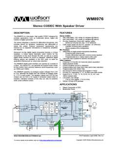
Pre-Production
WM8976
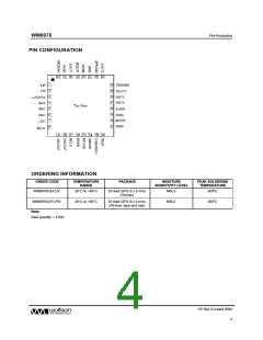
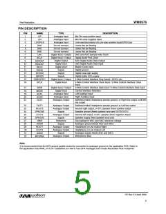
PIN DESCRIPTION
PIN
1
NAME
LIP
TYPE
Analogue input
Analogue input
Analogue input
Do not connect
Do not connect
Do not connect
Digital Input / Output
Digital Input / Output
Digital Output
Digital Input
DESCRIPTION
Mic Pre-amp positive input
Mic Pre-amp negative input
2
LIN
3
L2/GPIO2
DNC
Line input/secondary mic pre-amp positive input/GPIO2 pin
Leave this pin floating
4
5
DNC
Leave this pin floating
6
DNC
Leave this pin floating
7
LRC
DAC and ADC Sample Rate Clock
Digital Audio Port Clock
8
BCLK
9
ADCDAT
DACDAT
MCLK
ADC Digital Audio Data Output
DAC Digital Audio Data Input
Master Clock Input
10
11
12
13
14
15
16
Digital Input
DGND
DCVDD
DBVDD
CSB/GPIO1
SCLK
Supply
Digital ground
Supply
Digital core logic supply
Supply
Digital buffer (I/O) supply
Digital Input / Output
Digital Input
3-Wire Control Interface Chip Select / GPIO1 pin
3-Wire Control Interface Clock Input / 2-Wire Control Interface Clock
Input
17
18
19
20
21
SDIN
MODE
AUXL
AUXR
OUT4
Digital Input / Output
Digital Input
3-Wire Control Interface Data Input / 2-Wire Control Interface Data Input
Control Interface Selection
Analogue input
Analogue input
Analogue Output
Left Auxillary input
Right Auxillary input
Buffered midrail Headphone pseudo-ground, or Right line output or MONO
mix output
22
23
24
25
26
27
28
29
30
31
32
OUT3
ROUT2
SPKGND
LOUT2
SPKVDD
VMID
Analogue Output
Analogue Output
Supply
Buffered midrail Headphone pseudo-ground, or Left line output
Second right output, or BTL speaker driver positive output
Speaker ground (feeds speaker amp and OUT3/OUT4)
Second left output, or BTL speaker driver negative output
Speaker supply (feed speaker amp only)
Decoupling for ADC and DAC reference voltage
Analogue ground (feeds ADC and DAC)
Headphone or Line Output Right
Analogue Output
Supply
Reference
AGND
Supply
ROUT1
LOUT1
AVDD
Analogue Output
Analogue Output
Supply
Headphone or Line Output Left
Analogue supply (feeds ADC and DAC)
MICBIAS
Analogue Output
Microphone Bias
Note:
It is recommended that the QFN ground paddle should be connected to analogue ground on the application PCB. Refer to
the application note WAN_0118 on “Guidelines on How to Use QFN Packages and Create Associated PCB Footprints”
PP Rev 3.0 April 2006
w
5

 WOLFSON [ WOLFSON MICROELECTRONICS PLC ]