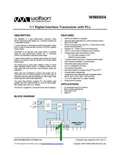
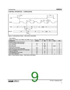
WM8804
Production Data
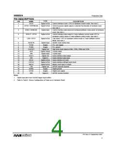
PIN DESCRIPTION
TYPE
PIN
NAME
DESCRIPTION
1
SCLK
Digital In/Out
Digital In/Out
Control interface clock / GPO in hardware control mode. See note 2.
2
GPO0 / SWIFMODE
General purpose digital output or selected functionality at hardware reset.
See note 2.
3
4
5
SDIN / HWMODE
SDOUT / GPO2
CSB / GPO1
Digital Input
Digital In/Out
Digital In/Out
Control interface data input and hardware/software mode select at hardware
reset. See note 2.
Control interface data output in 3-wire software control mode/ GPO in
hardware control mode or 2-wire software control mode. See note 2.
Chip select / GPO in hardware control mode or 2-wire software control
Mode. See note 2
6
RESETB
PVDD
PGND
CLKOUT
XOP
Digital Input
Supply
System reset (active low)
7
PLL core supply
8
Supply
PLL ground
9
Digital Out
Digital Output
Digital Input
Digital Out
Digital In
High drive clock output at 64fs, 128fs, 256fs and 512fs
Crystal output
10
11
12
13
14
15
16
17
18
19
20
XIN
Crystal input
DOUT
DIN
Audio interface data output
Audio interface data input
BCLK
LRCLK
MCLK
TX0
Digital In/Out
Digital In/Out
Digital In/Out
Digital Out
Supply
Audio interface bit clock
Audio interface left/right word clock
Master clock input or output
S/PDIF transmit channel
DGND
DVDD
RX0
Digital ground
Supply
Digital core supply
Digital In
S/PDIF receive channel
Notes:
1. Digital input pins have Schmitt trigger input buffers.
2. Refer to Table 6 Device Configuration at Power up or Hardware Reset
PD Rev 4.1 September 2007
4
w

 WOLFSON [ WOLFSON MICROELECTRONICS PLC ]