Production Data
WM8524
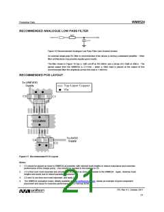
RECOMMENDED ANALOGUE LOW PASS FILTER
Figure 16 Recommended Analogue Low Pass Filter (one channel shown)
An external single-pole RC filter is recommended if the device is driving a wideband amplifier. Other
filter architectures may provide equally good results.
The filter shown in Figure 16 has a -3dB cut-off at 105.26kHz and a droop of 0.15dB at 20kHz. The
typical output from the WM8524 is 2.1Vrms – when a 10kΩ load is placed at the output of this
recommended filter the amplitude across this load is 1.99Vrms.
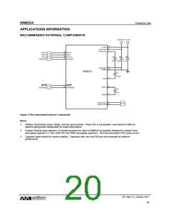
RECOMMENDED PCB LAYOUT
To LINEVDD
Supply
Top Layer Copper
Via
C2
C1
C5
W M 8 5 2 4
To AVDD
Supply
C4
C3
Figure 17 Recommended PCB Layout
Notes:
1. C5 should be placed as close to WM8524 as possible, with minimal track lengths to reduce inductance and maximise
performance of the charge pump. Vias should be avoided in the tracking to C5.
2. C1 is then next most important and should also be placed as close as possible to the WM8524. Again, minimise track
lengths and avoid vias to reduce parasitic inductance.
3. C2 and C4 are then next most important, and lastly C3.
4. The WM8524 evaluation board, details available at www.wolfsonmicro.com, shows an example of good component
placement and layout to maximise performance with a minimal BOM.
PD, Rev 4.1, October 2011
21
w

 WOLFSON [ WOLFSON MICROELECTRONICS PLC ]