WFF730
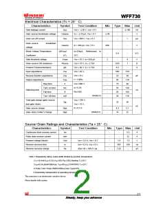
Electrical Characteristics (Tc = 25°C)
Characteristics
Symbol
IGSS
Test Condition
VGS = ±30 V, VDS = 0 V
IG = ±10 μA, VDS = 0 V
Min
-
Type Max Unit
Gate leakage current
-
±100
nA
Gate−source breakdown voltage
Drain cut−off current
V(BR)GSS
±30
-
-
V
IDSS
VDS = 400 V, VGS = 0 V
ID = 250 μA, VGS = 0 V
-
-
-
1
-
μA
V
Drain−source
voltage
breakdown
V(BR)DSS
400
Break Voltage Temperature
Coefficient
ΔBVDSS/
ΔTJ
VGS(th)
RDS(ON)
gfs
ID=250μA, Referenced to
25℃
-
0.4
-
V/℃
Gate threshold voltage
Drain−source ON resistance
Forward Transconductance
Input capacitance
VDS = 10 V, ID =250 μA
VGS = 10 V, ID = 2.75A
VDS = 50 V, ID = 2.75A
VDS = 25 V,
2
-
-
-
-
-
-
-
-
-
-
4
V
Ω
S
0.83
4.5
550
23
1
-
Ciss
720
30
VGS = 0 V,
Reverse transfer capacitance
Output capacitance
Crss
Coss
tr
pF
ns
f = 1 MHz
85
110
40
Rise time
VDD =200 V,
ID =5.5A
15
Turn−on time
Switching time
ton
55
120
180
110
RG=25Ω
Fall time
tf
85
(Note4,5)
Turn−off time
Total gate charge (gate−source
plus gate−drain)
toff
50
VDD = 320 V,
VGS = 10 V,
ID =5.5 A
Qg
-
32
38
nC
Gate−source charge
Qgs
Qgd
-
-
4.3
14
5.7
22
(Note4,5)
Gate−drain (“miller”) Charge
Source−Drain Ratings and Characteristics (Ta = 25°C)
Characteristics
Continuous drain reverse current
Pulse drain reverse current
Forward voltage (diode)
Symbol
Test Condition
Min Type Max Unit
IDR
IDRP
VDSF
trr
-
-
-
-
-
-
-
5.5
22
1.5
530
-
A
-
-
A
IDR = 5.5 A, VGS = 0 V
1.4
265
2.32
V
Reverse recovery time
ns
μC
IDR = 5.5 A, VGS = 0 V,
dIDR / dt = 100 A / μs
Reverse recovery charge
Qrr
Note 1.Repeativity rating :pulse width limited by junction temperature
2.L=18.5mH,IAS=5.5A,VDD=50V,RG=25Ω,Starting TJ=25℃
3.ISD≤5.5A,di/dt≤300A/us, VDD<BVDSS,STARTING TJ=25℃
4.Pulse Test: Pulse Width≤300us,Duty Cycle≤2%
5.Essentially independent of operating temperature.
This transistor is an electrostatic sensitive device
Please handle with caution
2/7
Steady, keep you advance

 WINSEMI [ SHENZHEN WINSEMI MICROELECTRONICS CO., LTD ]