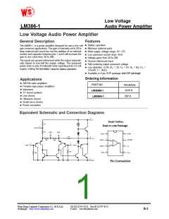
LM386-1
Application Hints
GAIN CONTROL
INPUT BIASING
a more versatile amplifier, two pins (1
The schematic shows that both inputs are biased to ground
with a 50 kΩ resistor. The base current of the input transis-
tors is about 250 nA, so the inputs are at about 12.5 mV
when left open. If the dc source resistance driving the LM386
is higher than 250 kΩ it will contribute very little additional
offset (about 2.5 mV at the input, 50 mV at the output). If the
dc source resistance is less than 10 kΩ, then shorting the
unused input to ground will keep the offset low (about 2.5 mV
at the input, 50 mV at the output). For dc source resistances
between these values we can eliminate excess offset by put-
ting a resistor from the unused input to ground, equal in
value to the dc source resistance. Of course all offset prob-
lems are eliminated if the input is capacitively coupled.
To make LM386-1
and 8) are provided for gain control. With pins 1 and 8 open
the 1.35 kΩ resistor sets the gain at 20 (26 dB). If a capacitor
is put from pin 1 to 8, bypassing the 1.35 kΩ resistor, the
gain will go up to 200 (46 dB). If a resistor is placed in series
with the capacitor, the gain can be set to any value from 20
to 200. Gain control can also be done by capacitively cou-
pling a resistor (or FET) from pin 1 to ground.
Additional external components can be placed in parallel
with the internal feedback resistors to tailor the gain and fre-
quency response for individual applications. For example,
we can compensate poor speaker bass response by fre-
quency shaping the feedback path. This is done with a series
RC from pin 1 to 5 (paralleling the internal 15 kΩ resistor).
For 6 dB effective bass boost: R . 15 kΩ, the lowest value
for good stable operation is R = 10 kΩ if pin 8 is open. If pins
1 and 8 are bypassed then R as low as 2 kΩ can be used.
This restriction is because the amplifier is only compensated
for closed-loop gains greater than 9.
with higher gains (bypassing the
When using LM386-1
1.35 kΩ resistor between pins 1 and 8) it is necessary to by-
pass the unused input, preventing degradation of gain and
possible instabilities. This is done with a 0.1 µF capacitor or
a short to ground depending on the dc source resistance on
the driven input.
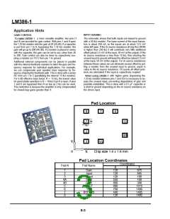
Pad Location
8
7
6
90
1
90
5
2
3
4B
4A
Y
X
0
Chip size 1.4 x 1.6 mm
Pad Location Coordinates
Coordinates
Pad N
Pad Name
X
Y
1
2
3
4A
4B
5
6
7
8
Gain
-input
+input
GND
GND
VOUT
VCC
BYPASS
Gain
120
120
120
550
600
600
750
440
120
975
665
100
100
390
1015
1405
1405
1405
8-3

 Wing Shing [ WING SHING COMPUTER COMPONENTS ]