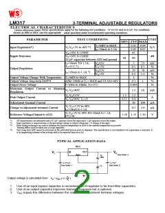
3-TERMINAL ADJUSTABLE REGULATORS
ELECTRICAL CHARACTERISTICS
,these specifications apply for the following test conditions:
Vi-Vo=5V and Io=0.5A. For conditions
Uniess otherwise noted
shown as MIN or MAX, use the appropriate
value specified under recommended operating conditions.
PARAMETER
TEST CONDITIONS
UNIT
MIN TYP MAX
0.01 0.04
0.02 0.07
65
TJ=MIN to MAX
IO=10mA to 1.5A
Input Regulation*2
Ripple Rejection
VI-VO=3V to 40V *3
%/V
VO=10V, f=120HZ
VO=10V, f=120HZ
10-µF capacitor between ADJ and ground
dB
66
80
IO=10mA TO 1.5A,
TJ=25℃*3,
VO≤5V
VO>5V
VO≥5V
VO>5V
5
0.1
20
25
0.5
70
mV
%
mV
%
Output Regulation
IO=10mA to 1.5A *3
0.3
1
1.5
Output Voltage Change With Temperature TJ=MIN to MAX
%
Output Voltage long-term Drift*4
Output Noise Voltage
After 1000h at TJ = MAX and VI-VO=40V
f=10Hz to 10kHz, TJ=25℃
0.3
0.003
1
%
%
Minimum Output Current to Maintain
Regulation
VI-VO=40V
3.5
2.2
0.15 0.4
50
10
mA
VI-VO≤15V
VI-VO≤40V, TJ=25
1.5
Peak Output Current
A
Adjustment-terminal Current
Change in adjustment-terminal Current
100
5.0
µA
µA
VI-VO=2.5V to 40V,
IO=10mA to 1.5A
0.2
V
-
I VO=3V to 40V, IO=10mA to 1.5A,
Reference Voltage(Output to ADJ)
1.20 1.25 1.30
V
P≤15W
*1
*2
*3
All characteristics are measured with a 0.1-µF capacitor across the input and a 1-µF capacitor across the output.
Input regulation is expressed here as the percentage change in output voltage per 1-V change at the input
Pulse testing techniques are used to maintain the junction temperature as close to the ambient temperature as possible.
Thermal effects must be taken into account separately.
*4
Since long-term drift cannot be measured on the individual devices prior to shipment. This specification is not intended to be a guarantee or warranty. It
is an engineering estimate of the average drift to be expected from lot to lot.
TYPICAL APPLICATION DATA
REG
OUT
IN
V0
VI
ADJ
See Note 3
R1
240
C2=1
F
C1=0.1
F
See Note 1
See Note 2
R2
R2
Output voltage is calculated from
VO = VREF { 1+
}
R1
1. Use of an input bypass capacitor is recommended if regulator is far from filter capacitors.
2. Use of an output capacitor improves transient response but is optional.
3. VREF equals the difference between the output and adjustment terminal voltages.

 Wing Shing [ WING SHING COMPUTER COMPONENTS ]