ꢀ
ꢀ
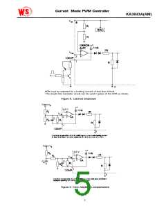
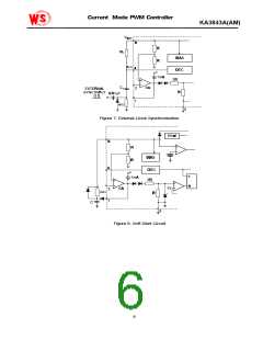
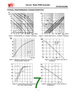
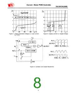
ꢀꢀꢀꢀꢀꢀꢀꢀꢀꢀCurrentꢀꢀModeꢀPWMꢀControllerꢀ
KA3843A(AM)
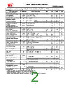
Electrical characteristics (*VCC=15V, RT=10kΩ, CT=3.3nF, TA=00C to +700C, unless otherwise
specified)
Characteristics
Reference Section
Reference Output Voltage
Line Regulation
Symbol
Test Condition
Min
Typ
Max
Unit
VREF
4.9
5.0
6.0
5.1
20
V
TJ = 25°C, IREF = 1 mA
12V ≤ VCC ≤ 25 V
1 mA ≤ IREF ≤ 20mA
TA = 25°C
mV
∆VREF
∆VREF
ISC
Load Regulation
6.0
25
Short Circuit Output Current
Oscillator Section
-100
-180
mA
f
384XA
47
47
50
52
57
57
TJ = 25°C
Oscillation Frequency
KHz
384XAM
Frequency Change with
Voltage
0.05
1.0
∆f/∆VCC
12V ≤ VCC ≤ 25 V
%
V
Oscillator Amplitude
Error Amplifier Section
Input Bias Current
V(OSC)
(peak to peak)
1.6
IBIAS
VI(E.A)
AVOL
VFB=3V
-0.1
2.5
90
-2
µA
Input Voltage
Vpin1 = 2.5V
2.42
65
2.58
V
Open Loop Voltage Gain
Power Supply Rejection Ratio
Output Sink Current
Output Source Current
High Output Voltage
Low Output Voltage
Current Sense Section
Gain
2V ≤ V0 ≤ 4V
dB
PSRR
ISINK
60
70
12V ≤ VCC ≤ 25 V
Vpin2 = 2.7V, Vpin1 = 1.1V
Vpin2 = 2.3V, Vpin1 = 5V
Vpin2 = 2.3V, RL = 15KΩ to GND
Vpin2 = 2.7V, RL = 15KΩ to PIN 8
2
7
mA
mA
ISOURCE
VOH
-0.5
5.0
-1.0
6.0
0.8
V
VOL
1.1
GV
VI(MAX)
SVR
(Note 1 & 2)
2.85
0.9
3.0
1.0
70
3.15
1.1
V/V
V
Maximum Input Signal
Supply Voltage Rejection
Input Bias Current
V pin1 = 5V (Note1)
12V ≤ VCC ≤ 25 V (Note 1)
Vpin3 = 3V
dB
IBIAS
-3.0
-10
µA
Output Section
Low Output Voltage
VOL
VOH
ISINK = 20 mA
0.08
1.4
0.4
2.2
ISINK = 200 mA
V
High Output Voltage
ISINK = 20 mA
13
12
13.5
13.0
45
ISINK = 200 mA
Rise Time
tR
tF
150
150
TJ = 25°C, CL = 1nF (Note 3)
TJ = 25°C, CL = 1nF (Note 3)
nS
Fall Time
35
Undervoltage Lockout Section
Start Theshold
VTH(ST)
V
V
3843A(AM)
7.8
7.0
95
8.4
7.6
97
9.0
8.2
100
0
Min. Operating Voltage
(After Turn On)
VOPR(min)
3843A(AM)/45A(AM)
3842A(AM)/43A(AM)
PWM Section
Max. Duty Cycle
D(MAX)
D(MAX)
%
Min. Duty Cycle
Total Standby Current
Start−Up Current
IST
ICC (OPR)
VZ
384XA(AM)
Vpin3 = Vpin2 = 0V
ICC=25 mA
0.17
13
0.3
17
mA
V
Operating Supply Current
Zener Voltage
30
38
* Adjust VCC above the start threshold before setting it to 15V.
Note 1: Parameter measured at trip point of latch with Vpin2=0.
Note 2: Gain defined as A=∆Vpin1/∆Vpin3 ; 0 ≤ Vpin3 ≤ 0.8V.
Note 3: These parameters, although guaranteed, are not 100% tested in production.
2

 Wing Shing [ WING SHING COMPUTER COMPONENTS ]