W90N745CD/W90N745CDG
Continued.
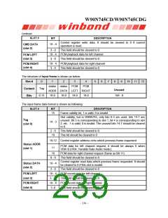
SLOT #
BIT
19 - 4
3 - 0
DESCRIPTION
Control register write data. It should be cleared to 0 if current
operation is read.
CMD DATA
(slot 2)
This field should be cleared to 0
19 - 4 PCM playback data for left channel
3 - 0 This field should be cleared to 0
19 - 4 PCM playback data for right channel
3 - 0 This field should be cleared to 0
PCM LEFT
(slot 3)
PCM RIGHT
(slot 4)
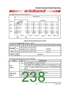
The structure of input frame is shown as below:
0
1
2
3
4
5
6
7
8
9
10 11 12
Slot #
Content
Bits
status status
PCM
PCM
Tag
0-15
Unused
ADDR DATA LEFT RIGHT
19-0 19-0 19-0 19-0
159 - 0
The input frame data format is shown as following:
SLOT #
BIT
DESCRIPTION
Frame validity bit, 1 is valid, 0 is invalid.
15
Slot validity, but in W90N745, only bits 6-3 are used, bits 14-7 are
unused. Bit 3 is corresponding to slot 1, bit 4 is corresponding to slot
2, etc.. 1 is valid, 0 is invalid. The unused bits 14-7 should be cleared
to 0.
Tag
14 - 3
(slot 0)
2 - 0
19
This field should be cleared to 0.
This bit should be cleared to 0
18-12 Control register address echo which previous frame requested
Status ADDR
(slot 1)
PCM data for left channel request, it should be always 0 when
VRA=0 (VRA: Variable Rate Audio mode).
11
10
PCM data for right channel request (Same as Bit 11).
This field should be cleared to 0
9 - 0
Control register read data which previous frame requested. It should
be cleared to 0 if this slot is invalid.
Status DATA
(slot 2)
19 - 4
3 - 0
This field should be cleared to 0
19 - 4 PCM record data for left channel
3 - 0 This field should be cleared to 0
19 - 4 PCM record data for right channel
PCM LEFT
(slot 3)
PCM RIGHT
(slot 4)
3 -0
This field should be cleared to 0
- 234 -

 WINBOND [ WINBOND ]