W90N745CD/W90N745CDG
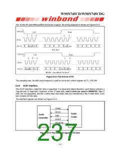
The signal format is shown as Figure 6.9.4
Frame (48 KHz)
Data phase
Tag phase
12.288 MHz
SYN
.
.
.
BCL
DIN
.
.
.
.
.
.
.
.
.
.
.
.
.
.
.
DOU
B255
B0 B1
B15 B16
B35 B36
B55 B56
B75 B76
B95 B96
B255
Slot 0
Slot 1
Slot 2
Slot 4
Slot 5 –12
Slot 3
MS
LS
Figure 6.9.4 The signal format of AC-link
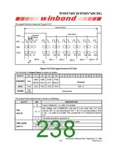
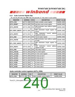
The structure of output frame is shown as below:
SLOT #
0
1
2
3
4
5
6
7
8
9
10
11
12
CMD CMD PCM PCM
ADDR DATA LEFT RIGHT
CONTENT Tag
Unused
BITS
15-0
19-0
19-0
19-0
19-0
159 - 0
Tag
phase
PHASE
Data phase
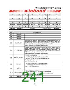
The output frame data format is shown as following:
SLOT #
BIT
DESCRIPTION
15
Frame validity bit, 1 is valid, 0 is invalid.
Slot validity, but in W90N745, only bits 6-3 are used, bits 14-7 are
unused. Bit 3 is corresponding to slot 1, bit 4 is corresponding to slot
2, etc.. 1 is valid, 0 is invalid. The unused bits 14-7 should be cleared
to 0.
Tag
14 - 3
(slot 0)
2 - 0
19
This field should be cleared to 0.
Read/write control, 1 for read and 0 for write
CMD ADDR
(slot 1)
18-12 Control register address
11 - 0 This field should be cleared to 0
Publication Release Date: September 22, 2006
Revision A2
- 233 -

 WINBOND [ WINBOND ]