W25Q80BV
9.2.38 Program Security Registers (42h)
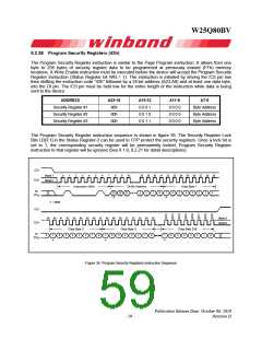
The Program Security Register instruction is similar to the Page Program instruction. It allows from one
byte to 256 bytes of security register data to be programmed at previously erased (FFh) memory
locations. A Write Enable instruction must be executed before the device will accept the Program Security
Register Instruction (Status Register bit WEL= 1). The instruction is initiated by driving the /CS pin low
then shifting the instruction code “42h” followed by a 24-bit address (A23-A0) and at least one data byte,
into the DI pin. The /CS pin must be held low for the entire length of the instruction while data is being
sent to the device.
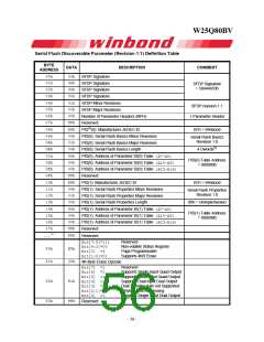
ADDRESS
A23-16
00h
A15-12
0 0 0 1
0 0 1 0
0 0 1 1
A11-8
0 0 0 0
0 0 0 0
0 0 0 0
A7-0
Security Register #1
Security Register #2
Security Register #3
Byte Address
Byte Address
Byte Address
00h
00h
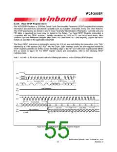
The Program Security Register instruction sequence is shown in figure 36. The Security Register Lock
Bits LB[3:1] in the Status Register-2 can be used to OTP protect the security registers. Once a lock bit is
set to 1, the corresponding security register will be permanently locked, Program Security Register
instruction to that register will be ignored (See 9.1.9, 9.2.21 for detail descriptions).
/CS
Mode 3
Mode 0
0
1
2
3
4
5
6
7
8
9
10
28 29 30 31 32 33 34 35 36 37 38 39
CLK
Instruction (42h)
24-Bit Address
Data Byte 1
DI
(IO0)
23 22 21
3
2
1
0
7
6
5
4
3
2
1
0
*
*
= MSB
*
/CS
39 40 41 42 43 44 45 46 47 48 49 50 51 52 53 54 55
Mode 3
Mode 0
CLK
Data Byte 2
Data Byte 3
Data Byte 256
DI
(IO0)
0
7
6
5
4
3
2
1
0
7
6
5
4
3
2
1
0
7
6
5
4
3
2
1
0
*
*
*
Figure 36. Program Security Registers Instruction Sequence
Publication Release Date: October 06, 2010
Revision D
- 59 -

 WINBOND [ WINBOND ]