W25Q80BV
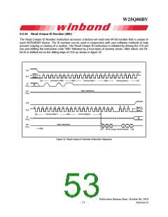
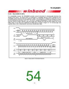
9.2.35 Read JEDEC ID (9Fh)
For compatibility reasons, the W25Q80BV provides several instructions to electronically determine the
identity of the device. The Read JEDEC ID instruction is compatible with the JEDEC standard for SPI
compatible serial memories that was adopted in 2003. The instruction is initiated by driving the /CS pin
low and shifting the instruction code “9Fh”. The JEDEC assigned Manufacturer ID byte for Winbond (EFh)
and two Device ID bytes, Memory Type (ID15-ID8) and Capacity (ID7-ID0) are then shifted out on the
falling edge of CLK with most significant bit (MSB) first as shown in figure 33. For memory type and
capacity values refer to Manufacturer and Device Identification table.
/CS
Mode 3
Mode 0
0
1
2
3
4
5
6
7
8
9
10 11 12 13 14 15
CLK
Instruction (9Fh)
High Impedance
DI
(IO0)
Manufacturer ID (EFh)
DO
(IO1)
= MSB
*
/CS
15 16 17 18 19 20 21 22 23 24 25 26 27 28 29 30
Mode 3
Mode 0
CLK
DI
(IO0)
Memory Type ID15-8
Capacity ID7-0
DO
(IO1)
7
6
5
4
3
2
1
0
7
6
5
4
3
2
1
0
*
*
Figure 33. Read JEDEC ID Instruction Sequence
- 54 -

 WINBOND [ WINBOND ]