W25Q20BW
1. GENERAL DESCRIPTION
The W25Q20BW (2M-bit) Serial Flash memory provides a storage solution for systems with limited
space, pins and power. The 25Q series offers flexibility and performance well beyond ordinary Serial
Flash devices. They are ideal for code shadowing to RAM, executing code directly from Dual/Quad SPI
(XIP) and storing voice, text and data. The device operates on a single 1.65V to 1.95V power supply with
current consumption as low as 4mA active and 1µA for power-down. All devices are offered in space-
saving packages.
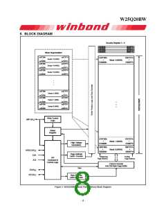
The W25Q20BW array is organized into 1,024 programmable pages of 256-bytes each. Up to 256 bytes
can be programmed at a time. Pages can be erased in groups of 16 (4KB sector erase), groups of 128
(32KB block erase), groups of 256 (64KB block erase) or the entire chip (chip erase). The W25Q20BW
has 64 erasable sectors and 4 erasable blocks respectively. The small 4KB sectors allow for greater
flexibility in applications that require data and parameter storage. (See figure 2.)
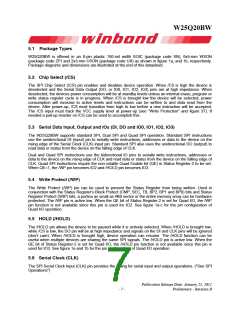
The W25Q20BW supports the standard Serial Peripheral Interface (SPI), and a high performance
Dual/Quad output as well as Dual/Quad I/O SPI: Serial Clock, Chip Select, Serial Data I/O0 (DI), I/O1
(DO), I/O2 (/WP), and I/O3 (/HOLD). SPI clock frequencies of up to 80MHz are supported allowing
equivalent clock rates of 160MHz (80MHz x 2) for Dual I/O and 320MHz (80MHz x 4) for Quad I/O when
using the Fast Read Dual/Quad I/O instructions. These transfer rates can outperform standard
Asynchronous 8 and 16-bit Parallel Flash memories. The Continuous Read Mode allows for efficient
memory access with as few as 8-clocks of instruction-overhead to read a 24-bit address, allowing true
XIP (execute in place) operation.
A Hold pin, Write Protect pin and programmable write protection, with top, bottom or complement array
control, provide further control flexibility. Additionally, the device supports JEDEC standard manufacturer
and device identification with a 64-bit Unique Serial Number.
2. FEATURES
• Family of SpiFlash Memories
– W25Q20BW: 2M-bit/256K-byte (262,144)
– 256-byte per programmable page
– Standard SPI: CLK, /CS, DI, DO, /WP, /Hold
– Dual SPI: CLK, /CS, IO0, IO1, /WP, /Hold
– Quad SPI: CLK, /CS, IO0, IO1, IO2, IO3
• Low Power, Wide Temperature Range
– Single 1.65 to 1.95V supply
– 4mA active current, <1µA Power-down current
– -40°C to +85°C operating range
• Flexible Architecture with 4KB sectors
– Uniform Sector Erase (4K-bytes)
– Uniform Block Erase (32K and 64K-bytes)
– Program one to 256 bytes
• Highest Performance Serial Flash
– 80MHz Dual/Quad SPI clocks
– 160/320MHz equivalent Dual/Quad SPI
– 40MB/S continuous data transfer rate
– Up to 6X that of ordinary Serial Flash
– More than 100,000 erase/program cycles
– More than 20-year data retention
– Erase/Program Suspend & Resume
• Advanced Security Features
– Software and Hardware Write-Protect
– Top/Bottom, 4KB complement array protection
– Lock-Down and OTP array protection(1)
– 64-Bit Unique Serial Number for each device
– 4X256-Byte Security Registers with OTP locks
– Volatile & Non-volatile Status Register Bits
• Efficient “Continuous Read Mode”
– Low Instruction overhead
– Continuous Read with 8/16/32/64-Byte Wrap
– As few as 8 clocks to address memory
– Allows true XIP (execute in place) operation
– Outperforms X16 Parallel Flash
• Space Efficient Packaging
– 8-pin SOIC 150-mil
– 8-pad WSON 6x5-mm, USON 2x3-mm
– Contact Winbond for KGD and other options
Note 1: Contact Winbond for details
Publication Release Date: January 25, 2011
Preliminary - Revision B
- 5 -

 WINBOND [ WINBOND ]