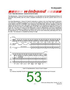
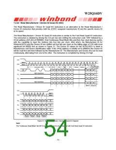
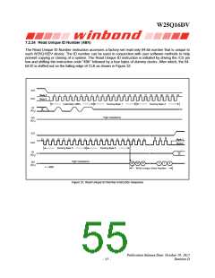
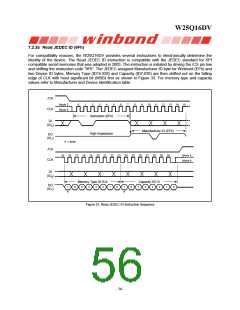
W25Q16DV
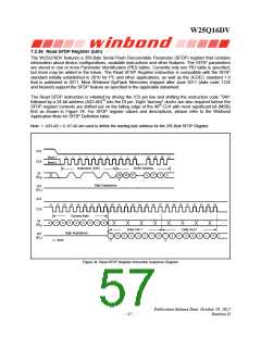
7.2.36 Read SFDP Register (5Ah)
The W25Q16DV features a 256-Byte Serial Flash Discoverable Parameter (SFDP) register that contains
information about device configurations, available instructions and other features. The SFDP parameters
are stored in one or more Parameter Identification (PID) tables. Currently only one PID table is specified,
but more may be added in the future. The Read SFDP Register instruction is compatible with the SFDP
standard initially established in 2010 for PC and other applications, as well as the JEDEC standard 1.0
that is published in 2011. Most Winbond SpiFlash Memories shipped after June 2011 (date code 1124
and beyond) support the SFDP feature as specified in the applicable datasheet.
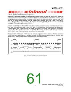
The Read SFDP instruction is initiated by driving the /CS pin low and shifting the instruction code “5Ah”
followed by a 24-bit address (A23-A0)(1) into the DI pin. Eight “dummy” clocks are also required before the
SFDP register contents are shifted out on the falling edge of the 40th CLK with most significant bit (MSB)
first as shown in Figure 34. For SFDP register values and descriptions, please refer to the Winbond
Application Note for SFDP Definition table.
Note: 1. A23-A8 = 0; A7-A0 are used to define the starting byte address for the 256-Byte SFDP Register.
/CS
Mode 3
Mode 0
0
1
2
3
4
5
6
7
8
9
10
28 29 30 31
CLK
Instruction (5Ah)
24-Bit Address
DI
(IO0)
23 22 21
3
2
1
0
*
High Impedance
DO
(IO1)
/CS
31 32 33 34 35 36 37 38 39 40 41 42 43 44 45 46 47 48 49 50 51 52 53 54 55
CLK
Dummy Byte
DI
(IO0)
0
7
6
5
4
3
2
1
0
Data Out 1
Data Out 2
High Impedance
DO
(IO1)
7
6
5
4
3
2
1
0
7
6
5
4
3
2
1
0
7
= MSB
*
*
*
Figure 34. Read SFDP Register Instruction Sequence Diagram
Publication Release Date: October 29, 2012
Revision D
- 57 -

 WINBOND [ WINBOND ]