W25Q16DV
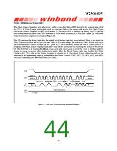
7.2.25 64KB Block Erase (D8h)
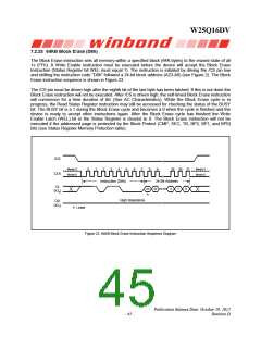
The Block Erase instruction sets all memory within a specified block (64K-bytes) to the erased state of all
1s (FFh). A Write Enable instruction must be executed before the device will accept the Block Erase
Instruction (Status Register bit WEL must equal 1). The instruction is initiated by driving the /CS pin low
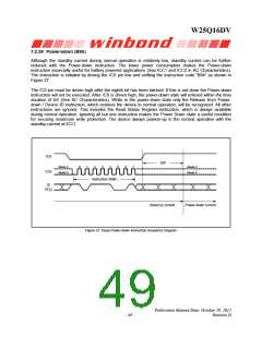
and shifting the instruction code “D8h” followed a 24-bit block address (A23-A0) (see Figure 2). The Block
Erase instruction sequence is shown in Figure 23.
The /CS pin must be driven high after the eighth bit of the last byte has been latched. If this is not done the
Block Erase instruction will not be executed. After /CS is driven high, the self-timed Block Erase instruction
will commence for a time duration of tBE (See AC Characteristics). While the Block Erase cycle is in
progress, the Read Status Register instruction may still be accessed for checking the status of the BUSY
bit. The BUSY bit is a 1 during the Block Erase cycle and becomes a 0 when the cycle is finished and the
device is ready to accept other instructions again. After the Block Erase cycle has finished the Write
Enable Latch (WEL) bit in the Status Register is cleared to 0. The Block Erase instruction will not be
executed if the addressed page is protected by the Block Protect (CMP, SEC, TB, BP2, BP1, and BP0)
bits (see Status Register Memory Protection table).
/CS
Mode 3
Mode 0
0
1
2
3
4
5
6
7
8
9
29 30 31
Mode 3
Mode 0
CLK
Instruction (D8h)
24-Bit Address
DI
(IO0)
23 22
2
1
0
*
High Impedance
DO
(IO1)
= MSB
*
Figure 23. 64KB Block Erase Instruction Sequence Diagram
Publication Release Date: October 29, 2012
Revision D
- 45 -

 WINBOND [ WINBOND ]