W25Q16DV
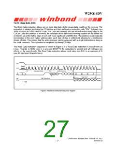
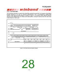
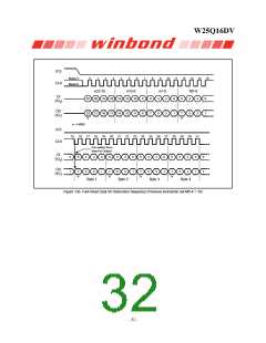
7.2.11 Fast Read (0Bh)
The Fast Read instruction is similar to the Read Data instruction except that it can operate at the highest
possible frequency of FR (see AC Electrical Characteristics). This is accomplished by adding eight
“dummy” clocks after the 24-bit address as shown in Figure 10. The dummy clocks allow the devices
internal circuits additional time for setting up the initial address. During the dummy clocks the data value
on the DO pin is a “don’t care”.
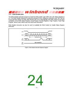
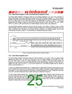
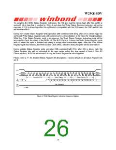
/CS
Mode 3
Mode 0
0
1
2
3
4
5
6
7
8
9
10
28 29 30 31
CLK
Instruction (0Bh)
24-Bit Address
DI
(IO0)
23 22 21
3
2
1
0
*
High Impedance
DO
(IO1)
= MSB
*
/CS
31 32 33 34 35 36 37 38 39 40 41 42 43 44 45 46 47 48 49 50 51 52 53 54 55
CLK
Dummy Clocks
DI
(IO0)
0
Data Out 1
Data Out 2
High Impedance
DO
(IO1)
7
6
5
4
3
2
1
0
7
6
5
4
3
2
1
0
7
*
*
Figure 10. Fast Read Instruction Sequence Diagram
- 28 -

 WINBOND [ WINBOND ]