WED3DG6432V-D1
White Electronic Designs
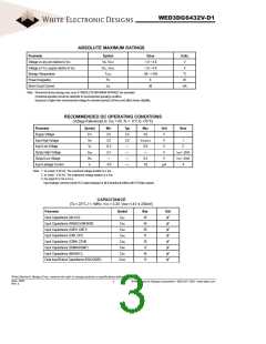
ABSOLUTE MAXIMUM RATINGS
Parameter
Symbol
Value
-1.0 ~ 4.6
-1.0 ~ 4.6
-55 ~ +150
8
Units
V
Voltage on any pin relative to VSS
Voltage on VCC supply relative to VSS
Storage Temperature
VIN, VOUT
VCC, VCCQ
TSTG
V
°C
W
Power Dissipation
PD
Short Circuit Current
IOS
50
mA
Note: Permanent device damage may occur if “ABSOLUTE MAXIMUM RATINGS” are exceeded.
Functional operation should be restricted to recommended operating condition.
Exposure to higher than recommended voltage for extended periods of time could affect device reliability.
RECOMMENDED DC OPERATING CONDITIONS
(Voltage Referenced to: VSS = 0V, TA = 0°C to +70°C)
Parameter
Symbol
VCC
VIH
Min
3.0
2.0
-0.3
2.4
—
Typ
3.3
3.0
—
Max
3.6
Unit
V
Note
Supply Voltage
Input High Voltage
Input Low Voltage
Output High Voltage
Output Low Voltage
Input Leakage Current
VCCQ+0.3
0.8
V
1
VIL
V
2
VOH
VOL
ILI
—
—
V
IOH= -2mA
IOL= -2mA
3
—
0.4
V
-10
—
10
µA
Note: 1. VIH (max)= 5.6V AC. The overshoot voltage duration is ≤ 3ns.
2. VIL (min)= -2.0V AC. The undershoot voltage duration is ≤ 3ns.
3. Any input 0V ≤ VIN ≤ VCCQ
Input leakage currents include Hi-Z output leakage for all bi-directional buffers with Tri-State outputs.
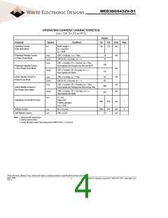
CAPACITANCE
(TA = 23°C, f = 1MHz, VCC = 3.3V, VREF=1.4V 200mV)
Parameter
Symbol
CIN1
Max
45
45
25
21
25
12
45
12
Unit
Input Capacitance (A0-A12)
pF
pF
pF
pF
pF
pF
pF
pF
Input Capacitance (RAS#,CAS#,WE#)
Input Capacitance (CKE0, CKE1)
Input Capacitance (CK0, CK1)
Input Capacitance (CS0#, CS1#)
Input Capacitance (DQM0-DQM7)
Input Capacitance (BA0-BA1)
Data Input/Output Capacitance (DQ0-DQ63)
CIN2
CIN3
CIN4
CIN5
CIN6
CIN7
CouT
White Electronic Designs Corp. reserves the right to change products or specifications without notice.
Sept. 2002
Rev. 0
3
White Electronic Designs Corporation • (602) 437-1520 • www.wedc.com

 WEDC [ WHITE ELECTRONIC DESIGNS CORPORATION ]