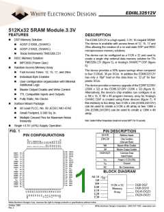
EDI8L32512V
White Electronic Designs
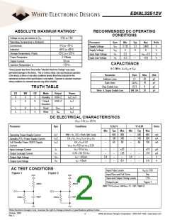
ABSOLUTE MAXIMUM RATINGS*
RECOMMENDED DC OPERATING
CONDITIONS
Voltage on any pin relative to VSS
Operating Temperature tA (Ambient)
Commercial
-0.5V to 7.0V
Parameter
Sym
VCC
VSS
VIH
Min
3.135
0
Typ
3.3
0
Max
3.465
0
Units
0°C to +70°C
-40°C to +85°C
-55°C to +125°C
2.5 Watts
Supply Voltage
Supply Voltage
Input High Voltage
Input Low Voltage
V
V
V
V
Industrial
Storage Temperature, Plastic
Power Dissipation
2.2
--
VCC + 0.3
+0.8
VIL
-0.3
--
Output Current
20 mA
CAPACITANCE
Junction Temperature, tJ
-175°C
(f=1.0MHz, VIN=VCC or VSS)
*Stress greater than those listed under "Absolute Maximum Ratings" may cause
permanent damage to the device. This is a stress rating only and functional operation
of the device at these or any other conditions greater than those indicated in the
operational sections of this specification is not implied. Exposure to absolute maximum
rating conditions for extended periods may affect reliability.
Parameter
Address Lines
Sym
CI
Max
30
10
8
Unit
pF
pF
pF
pF
Data Lines
CD/Q
E0-3
Chip Enable Line
TRUTH TABLE
Write & Output Enable Line
W#, G#
30
E#
H
W#
X
G#
X
Mode
Output
HIGH Z
HIGH Z
Power
ICC2, ICC
Standby
3
L
H
H
Output
ICC1
Deselect
L
L
H
L
L
Read
Write
DOUT
DIN
ICC
1
1
X
ICC
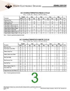
DC ELECTRICAL CHARACTERISTICS
(VCC= 3.3V, tA = 25°C)
Parameter
Sym
Conditions
12 & 15
17 & 20
Units
Min
--
Typ
440
100
60
Max
800
300
80
Min
Typ
440
100
60
Max
640
200
100
ICC1
ICC2
ICC3
W# = VIL, II/O = 0mA, Min Cycle
E# > VIH, VIN < VIL or VIN > VIH
--
--
--
mA
mA
mA
Operating Power Supply Current
--
Standby (TTL) Power Supply Current
Full Standby Power CMOS Supply
Current
E# > VCC-0.2V
VIN > VCC=0.2V or VIN < 0.2V
--
ILI
VIN = 0V to VCC
V I/O = 0V TO VCC
IOH = -4.0mA
--
--
--
--
--
--
±20
±20
--
--
--
--
--
--
--
±10
±10
--
µA
µA
V
Input Leakage Current
Output Leakage Current
Output High Voltage
Output Low Voltage
ILO
VOH
VOL
2.4
--
2.4
--
IOL = 4.0mA
0.4
0.4
V
AC TEST CONDITIONS
Input Pulse Levels
VSS to 3.0V
5ns
Figure 1
Figure 2
Input Rise and Fall Times
Input and Output Timing Levels
Output Load
Vcc
Vcc
1.5V
Figure 1
480Ω
480Ω
(Note: For tEHQZ,tGHQZ and tWLQZ, CL = 5pF, Figure 2)
Q
Q
30pF
5pF
255Ω
255Ω
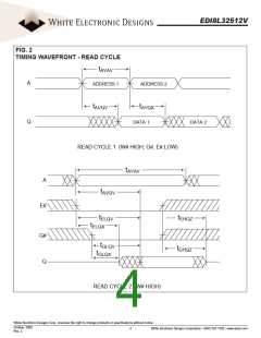
White Electronic Designs Corp. reserves the right to change products or specifications without notice.
October. 2000
Rev. 3
2
White Electronic Designs Corporation • (602) 437-1520 • www.wedc.com

 WEDC [ WHITE ELECTRONIC DESIGNS CORPORATION ]