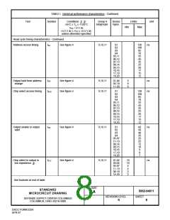
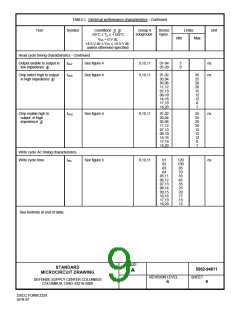
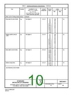
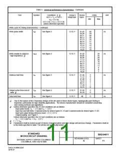
TABLE I. Electrical performance characteristics - Continued.
Test
Symbol
Conditions 1/ 2/
-55°C ≤ TC ≤ +125°C
Group A
subgroups
Device
types
Limits
Unit
Min
Max
VSS = 0 V dc
+4.5 V dc ≤ VCC ≤ +5.5 V dc
unless otherwise specified
Read cycle timing characteristics - Continued.
Address access timing
tAA
See figure 4
9,10,11
01
02
03
04
05,11
06,12
07,13
08,14
09,15
10,16
17,19
18,20
120
100
85
70
55
45
35
25
20
17
15
12
ns
Output hold from address
change
tOH
See figure 4
See figure 4
9,10,11
9,10,11
01-04
05-10
11-20
5
0
0
ns
ns
Chip select access timing
tACS
01
02
03
04
05,11
06,12
07,13
08,14
09,15
10,16
17,19
18,20
120
100
85
70
55
45
35
25
20
17
15
12
Output enable to output
valid
tOE
See figure 4
9,10,11
01
02
03
04
05-07
11-13
08,14
09,15
10,16
17,19
18,20
60
50
40
35
25
25
12
10
9
ns
8
7
Chip select to output in
low impedence 4/
tCLZ
See figure 4
9,10,11
01,02
03,04
05-07
11-13
08-10
14-20
10
10
4
4
2
ns
2
See footnote at end of table.
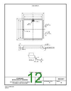
SIZE
STANDARD
MICROCIRCUIT DRAWING
5962-94611
A
REVISION LEVEL
SHEET
DEFENSE SUPPLY CENTER COLUMBUS
COLUMBUS, OHIO 43216-5000
8
R
DSCC FORM 2234
APR 97

 WEDC [ WHITE ELECTRONIC DESIGNS CORPORATION ]