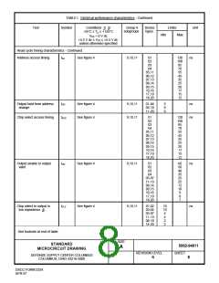
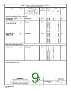
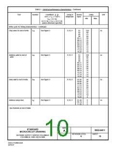
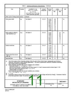
TABLE I. Electrical performance characteristics - Continued.
Test
Symbol
Conditions 1/ 2/
-55°C ≤ TC ≤ +125°C
Group A
subgroups
Device
types
Limits
Unit
Min
Max
VSS = 0 V dc
+4.5 V dc ≤ VCC ≤ +5.5 V dc
unless otherwise specified
Read cycle timing characteristics - Continued.
Output enable to output in
low impedence 4/
tOLZ
See figure 4
9,10,11
9,10,11
01-04
05-20
5
0
ns
Chip select high to output
in high impedence 4/
tCHZ
See figure 4
01,02
03,04
05,06
11,12
07,13
08-10
14-16
17,19
18,20
35
25
20
20
15
12
12
8
ns
7
Chip enable high to
output in high
impedence 4/
tOHZ
See figure 4
9,10,11
01,02
03,04
05,06
11,12
07,13
08-10
14-16
17,19
18,20
35
25
20
20
15
12
12
8
ns
7
Write cycle AC timing characteristics.
Write cycle time
tWC
See figure 5
9,10,11
01
02
03
04
05,11
06,12
07,13
08,14
09,15
10,16
17,19
18,20
120
100
85
70
55
45
35
25
20
17
15
12
ns
See footnote at end of table.
SIZE
STANDARD
MICROCIRCUIT DRAWING
5962-94611
A
REVISION LEVEL
SHEET
DEFENSE SUPPLY CENTER COLUMBUS
COLUMBUS, OHIO 43216-5000
9
R
DSCC FORM 2234
APR 97

 WEDC [ WHITE ELECTRONIC DESIGNS CORPORATION ]