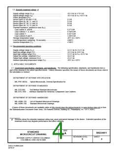
1.3 Absolute maximum ratings. 4/
Supply voltage range (VCC)........................................................
Signal voltage range (Vg)...........................................................
Power dissipation (PD):
-0.5 V dc to +7.0 V dc
-0.5 V dc to VCC +0.5 V dc
Device types 01-04 and 17-20...................................................
Device types 05, 06, 11, and 12................................................
Device types 07, 08, 13, and 14................................................
Device types 09, 10, 15, and 16................................................
Thermal resistance, junction-to-case (θJC):
2.2 W
3.2 W
3.6 W
4.4 W
Case outline A and M............................................................
Case outlines T, U, and X......................................................
Case outline Y........................................................................
Case outlines B and 9............................................................
Storage temperature range .......................................................
Lead temperature (soldering, 10 seconds)................................
Junction temperature (TJ)..........................................................
9.27°C/W
4.160°C/W
5.251°C/W
1.495°C/W
-65°C to +150°C
+300°C
+150°C
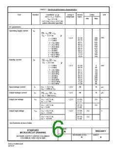
1.4 Recommended operating conditions.
Supply voltage range (VCC)........................................................
Input low voltage range (VIL)......................................................
Input high voltage range (VIH)....................................................
Output low voltage, maximum (VOL) ..........................................
Output high voltage, minimum (VOH) .........................................
Ambient operating temperature range (TA)................................
+4.5 V dc to +5.5 V dc
-0.3 V dc to +0.8 V dc
+2.2 V dc to VCC +0.3 V dc
+0.4 V dc
+2.4 V dc
-55°C to +125°C
2. APPLICABLE DOCUMENTS
2.1 Government specification, standards, and handbooks. The following specification, standards, and handbooks form a
part of this drawing to the extent specified herein. Unless otherwise specified, the issues of these documents are those cited in
the solicitation or contract.
DEPARTMENT OF DEFENSE SPECIFICATION
MIL-PRF-38534 - Hybrid Microcircuits, General Specification for.
DEPARTMENT OF DEFENSE STANDARDS
MIL-STD-883 - Test Method Standard Microcircuits.
MIL-STD-1835 - Interface Standard for Electronic Component Case Outlines.
DEPARTMENT OF DEFENSE HANDBOOKS
MIL-HDBK-103 - List of Standard Microcircuit Drawings.
MIL-HDBK-780 - Standard Microcircuit Drawings.
(Copies of these documents are available online at http://assist.daps.dla.mil/quicksearch/ or www.dodssp.daps.mil or from
the Standardization Document Order Desk, 700 Robbins Avenue, Building 4D, Philadelphia, PA 19111-5094.)
4/ Stresses above the absolute maximum rating may cause permanent damage to the device. Extended operation at the
maximum levels may degrade performance and affect reliability.
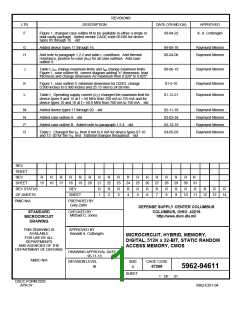
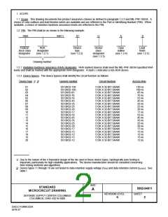
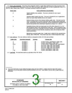
SIZE
STANDARD
5962-94611
A
MICROCIRCUIT DRAWING
REVISION LEVEL
SHEET
DEFENSE SUPPLY CENTER COLUMBUS
COLUMBUS, OHIO 43216-5000
4
R
DSCC FORM 2234
APR 97

 WEDC [ WHITE ELECTRONIC DESIGNS CORPORATION ]