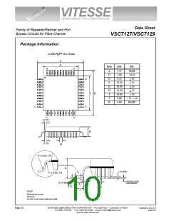
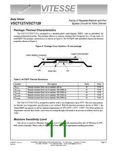
VITESSE
SEMICONDUCTOR CORPORATION
Data Sheet
Family of Repeater/Retimer and Port
Bypass Circuits for Fibre Channel
VSC7127/VSC7129
(1)
Absolute Maximum Ratings
TTL Power Supply Voltage (V )...................................................................................................... 0.5V to +4V
DD
PECL DC Input Voltage (V ) ............................................................................................. -0.5V to V +0.5V
INP
DD
TTL DC Input Voltage (V )........................................................................................................... -0.5V to 5.5V
INT
DC Voltage Applied to Outputs for High Output State (V
) ........................................ -0.5V to V + 0.5V
DD
IN TTL
TTL Output Current (I
), (DC, output high) ..........................................................................................+50mA
OUT
PECL Output Current, (I
), (DC, output high)........................................................................................-50mA
OUT
o
o
Case Temperature Under Bias (T )..............................................................................................-55 C to +125 C
C
o
o
Storage Temperature (T
)........................................................................................................-65 C to + 150 C
STG
Maximum Input ESD ................................................................................................................................... 1000V
(2)
Recommended Operating Conditions
Power Supply Voltage (V ) ....................................................................................................... +3.14V to 3.47V
DD
Ambient Operating Temperature Range (T)...............................................................0°C Ambient to +95°C Case
NOTES: (1) CAUTION: Stresses listed under “Absolute Maximum Ratings” may be applied to devices one at a time without causing permanent
damage. Functionality at or above the values listed is not implied. Exposure to these values for extended periods may affect device reli-
ability.
(2) Vitesse guarantees the functional and parametric operation of the part under “Recommended Operating Conditions” except where
specifically noted in the AC and DC Parametric tables.
© VITESSE SEMICONDUCTOR CORPORATION • 741 Calle Plano • Camarillo, CA 93012
G52298-0, Rev 4.3
05/01/01
Page 7
Tel: (800) VITESSE • FAX: (805) 987-5896 • Email: prodinfo@vitesse.com
Internet: www.vitesse.com

 VITESSE [ VITESSE SEMICONDUCTOR CORPORATION ]