VITESSE
SEMICONDUCTOR CORPORATION
Data Sheet
10-Bit Transceiver for Fibre
Channel and Gigabit Ethernet
VSC7123
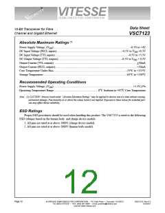
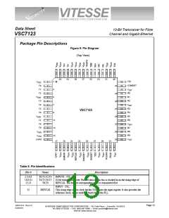
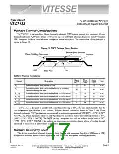
Package Pin Descriptions
Figure 9: Pin Diagram
(Top View)
63
61
59
57
55
53
51
49
TDI
1
VSSD
COMDET
47
T0
T1
3
VSST
R0
45
T2
VDDD
5
R1
R2
43
T3
T4
7
VDDT
R3
41
T5
T6
VSC7123
9
R4
VDDD
R5
R6
39
37
35
33
11
13
15
T7
T8
T9
VDDT
R7
R8
VSSD
VSSA
R9
VSST
CAP0
17
19
21
23
25
27
29
31
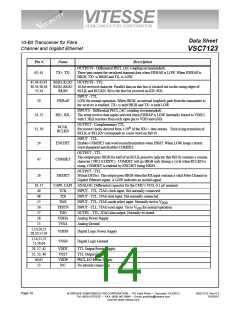
Table 5: Pin Identifications
Pin #
Name
Description
2,3,4,6
7,8,9,11
12,13
T0,T1,T2,T3
T4,T5,T6,T7
T8,T9
INPUTS - TTL:
10-bit transmit character. Parallel data on this bus is clocked in on the rising edge of
REFCLK. The data bit corresponding to T0 is transmitted first.
INPUT - TTL:
22
REFCLK
This rising edge of this clock latches T(0:9) into the input register. It also provides the
reference clock, at one tenth the baud rate to the PLL.
G52212-0, Rev 4.3
03/25//01
Page 13
© VITESSE SEMICONDUCTOR CORPORATION • 741 Calle Plano • Camarillo, CA 93012
Tel: (800) VITESSE • FAX: (805) 987-5896 • Email: prodinfo@vitesse.com
Internet: www.vitesse.com

 VITESSE [ VITESSE SEMICONDUCTOR CORPORATION ]