VITESSE
SEMICONDUCTOR CORPORATION
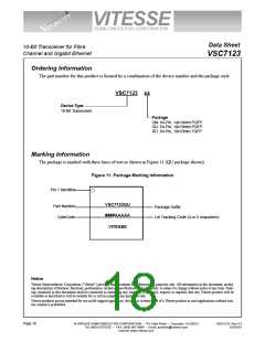
Data Sheet
10-Bit Transceiver for Fibre
Channel and Gigabit Ethernet
VSC7123
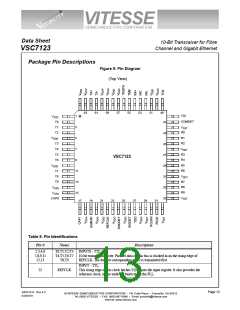
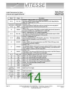
Pin #
Name
Description
OUTPUTS - Differential PECL (AC-coupling recommended):
62, 61
TX+, TX-
These pins output the serialized transmit data when EWRAP is LOW. When EWRAP is
HIGH, TX+ is HIGH and TX- is LOW.
45,44,43,41
40,39,38,36
35,34
R0,R1,R2,R3 OUTPUTS - TTL:
R4,R5,R6,R7 10-bit received character. Parallel data on this bus is clocked out on the rising edges of
R8,R9
RCLK and RCLKN. R0 is the first bit received on RX+/RX-.
INPUT - TTL:
19
EWRAP
LOW for normal operation. When HIGH, an internal loopback path from the transmitter to
the receiver is enabled. TX+ is held HIGH and TX- is held LOW.
INPUTS - Differential PECL (AC-coupling recommended):
54, 52
31, 30
24
RX+, RX-
The serial receive data inputs selected when EWRAP is LOW. Internally biased to VDD/2,
with 3.3KΩ resistors from each input pin to VDD and GND.
OUTPUT - Complementary TTL:
RCLK,
RCLKN
Recovered clocks derived from 1/20th of the RX+/- data stream. Each rising transition of
RCLK or RCLKN corresponds to a new word on R(0:9).
INPUT - TTL:
ENCDET
COMDET
SIGDET
Enables COMDET and word resynchronization when HIGH. When LOW, keeps current
word alignment and disables COMDET.
OUTPUT - TTL:
This output goes HIGH for half of an RCLK period to indicate that R(0:9) contains a comma
character (‘0011111XXX’). COMDET will go HIGH only during a cycle when RCLKN is
rising. COMDET is enabled by ENCDET being HIGH.
47
OUTPUT - TTL
26
SIGnal DETect. This output goes HIGH when the RX input contains a valid Fibre Channel or
Gigabit Ethernet signal. A LOW indicates an invalid signal.
16, 17
49
CAP0, CAP1 ANALOG: Differential capacitor for the CMU’s VCO, 0.1 µF nominal.
TCK
TDI
INPUT - TTL: JTAG clock input. Not normally connected.
INPUT - TTL: JTAG data input. Not normally connected.
INPUT - TTL: JTAG mode select input. Normally tied to VDDD
INPUT - TLL: JTAG reset input. Tie to VSSD for normal operation.
OUTPU - TTL: JTAG data output. Normally tri-stated.
Analog Power Supply
48
55
TMS
56
TRSTN
TDO
27
18
VDDA
VSSA
15
Analog Ground
5,10,20,23
28,50,57,59
VDDD
VSSD
Digital Logic Power Supply
Digital Logic Ground
1,14,21,25
51,58,64
29, 37, 42
32, 33, 46
60,63
VDDT
VSST
VDDP
N/C
TTL Output Power Supply
TTL Output Ground
PECL I/O Power Supply
No internal connection
53
© VITESSE SEMICONDUCTOR CORPORATION • 741 Calle Plano • Camarillo, CA 93012
Tel: (800) VITESSE • FAX: (805) 987-5896 • Email: prodinfo@vitesse.com
Internet: www.vitesse.com
Page 14
G52212-0, Rev 4.3
03/25/01

 VITESSE [ VITESSE SEMICONDUCTOR CORPORATION ]