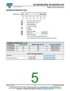
VS-30CPQ0.0PbF, VS-30CPQ0.0-N3
www.vishay.com
Vishay Semiconductors
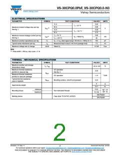
ELECTRICAL SPECIFICATIONS
PARAMETER
SYMBOL
TEST CONDITIONS
VALUES
0.60
0.80
0.56
0.70
0.80
45
UNITS
15 A
TJ = 25 °C
30 A
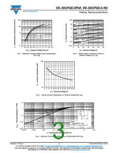
Maximum forward voltage drop per leg
See fig. 1
(1)
VFM
V
15 A
TJ = 125 °C
30 A
TJ = 25 °C
TJ = 125 °C
Maximum reverse leakage current per leg
See fig. 2
(1)
IRM
V
R = Rated VR
mA
Maximum junction capacitance per leg
Typical series inductance per leg
Maximum voltage rate of change
CT
LS
VR = 5 VDC (test signal range 100 kHz to 1 MHz) 25 °C
Measured lead to lead 5 mm from package body
Rated VR
720
pF
nH
7.5
dV/dt
10 000
V/µs
Note
(1)
Pulse width < 300 μs, duty cycle < 2 %
THERMAL - MECHANICAL SPECIFICATIONS
PARAMETER
SYMBOL
TEST CONDITIONS
VALUES
UNITS
Maximum junction and storage
temperature range
TJ, TStg
- 55 to 150
°C
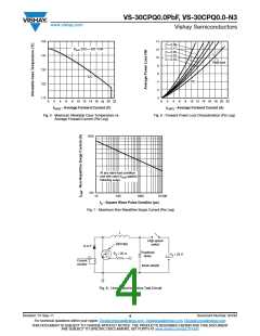
Maximum thermal resistance,
junction to case per leg
DC operation
See fig. 4
2.20
1.10
0.24
RthJC
Maximum thermal resistance,
junction to case per package
DC operation
°C/W
Typical thermal resistance,
case to heatsink
RthCS
Mounting surface, smooth and greased
6
g
Approximate weight
Mounting torque
Marking device
0.21
oz.
minimum
maximum
6 (5)
12 (10)
kgf cm
(lbf in)
Non-lubricated threads
30CPQ050
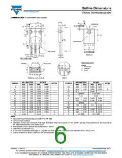
Case style TO-247AC (JEDEC)
30CPQ060
Revision: 01-Sep-11
Document Number: 94183
2
For technical questions within your region: DiodesAmericas@vishay.com, DiodesAsia@vishay.com, DiodesEurope@vishay.com
THIS DOCUMENT IS SUBJECT TO CHANGE WITHOUT NOTICE. THE PRODUCTS DESCRIBED HEREIN AND THIS DOCUMENT
ARE SUBJECT TO SPECIFIC DISCLAIMERS, SET FORTH AT www.vishay.com/doc?91000

 VISHAY [ VISHAY ]