New Product
SMB30A300
Vishay General Semiconductor
Asymmetric Transient Voltage Suppressor
FEATURES
• Glass passivated chip junction
• Ideal for automated placement
• Very fast response time
• Low incremental surge resistance, excellent
clamping capability
• Meets MSL level 1, per J-STD-020C, LF max peak
of 260 °C
• Solder dip 260 °C, 40 seconds
• Component in accordance to RoHS 2002/95/EC
and WEEE 2002/96/EC
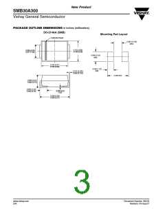
DO-214AA (SMB)
300 V
30 V
TYPICAL APPLICATIONS
For use in wiper motor application, to replace varistor.
MECHANICAL DATA
Case: DO-214AA (SMB)
Epoxy meets UL 94V-0 flammability rating
Terminals: Matte tin plated leads, solderable per
J-STD-002B and JESD22-B102D
PRIMARY CHARACTERISTICS
IPPM
14.5 A
VC
41.4 V
30 V
V
BR at TVS
VBR at Diode
TJ max.
300 V
150 °C
E3 suffix for commercial grade, HE3 suffix for high
reliability grade (AEC Q101 qualified)
Polarity: Color band denotes TVS 30 V cathode end,
the cathode of 300 V is at the other terminal side
MAXIMUM RATINGS (T = 25 °C unless otherwise noted)
A
PARAMETER
SYMBOL
IPPM
VALUE
14.5
UNIT
A
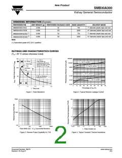
Peak pulse current with a 10/1000 µs waveform per (Fig. 1)
Maximum reverse current of 30 V TVS side at VWM = 25.6 V (1)(2)
Maximum reverse current of 300 V diode side at VWM = 243 V (1)(2)
Operating junction and storage temperature range
ID
5.0
µA
µA
°C
ID
1.0
TJ, TSTG
- 55 to + 150
Notes:
(1) All terms and symbols are consistant with ANSI/IEEE C62.35
(2) VWM means stand-off voltage
ELECTRICAL CHARACTERISTICS (T = 25 °C unless otherwise noted)
A
TYPICAL
JUNCTION
CURRENT CAPACITANCE AT
BREAKDOWN VOLTAGE
VBR
MAXIMUM PEAK
PULSE SURGE
MAXIMUM
CLAMPING
VOLTAGE
TEST
DEVICE
MARKING
CODE
DEVICE TYPE
AT IT (1) (V)
(2)
CURRENT IPPM
IT (mA)
4.0 V, 1 MHz
CJ (pF)
AT IPPM VC (V)
(A)
MIN
MAX
SMB30A300
30 V TVS
30F
28.5
270
31.5
360
1.0
1.0
130
72
14.5
-
41.4
-
300 V Diode
Notes:
(1) Pulse test: tp ≤ 50 ms
(2) Surge current waveform per Fig. 1
www.vishay.com
252
Document Number: 88476
Revision: 03-Aug-07

 VISHAY [ VISHAY ]