MBR(F,B)1090 & MBR(F,B)10100
Vishay General Semiconductor
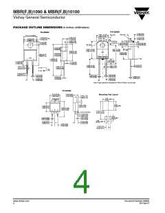
PACKAGE OUTLINE DIMENSIONS in inches (millimeters)
ITO-220AC
See note
TO-220AC
0.190 (4.83)
0.170 (4.32)
See note
0.404 (10.26)
0.384 (9.75)
0.076 Ref.
(1.93) ref.
0.415(10.54)MAX.
0.154(3.91)
0.185(4.70)
0.110 (2.79)
0.100 (2.54)
DIA.
0.370(9.40)
0.360(9.14)
0.148(3.74)
0.175(4.44)
0.055(1.39)
0.045(1.14)
7° Ref.
0.076 Ref.
0.113(2.87)
0.103(2.62)
(1.93) Ref.
0.140 (3.56) DIA.
0.125 (3.17) DIA.
0.135 (3.43) DIA.
0.122 (3.08) DIA.
45° Ref.
0.145(3.68)
0.135(3.43)
0.600 (15.24)
0.580 (14.73)
0.671 (17.04)
0.651 (16.54)
7° Ref.
0.603(15.32)
0.573(14.55)
PIN
0.350 (8.89)
0.330 (8.38)
0.350(8.89)
0.330(8.38)
0.635(16.13)
0.625(15.87)
2
1
Copper exposure
0.010 (0.25) Max.
PIN
7° Ref.
1
2
1.148(29.16)
1.118(28.40)
0.191 (4.85)
0.171 (4.35)
0.160(4.06)
0.140(3.56)
0.110(2.79)
0.100(2.54)
0.110 (2.79)
0.100 (2.54)
0.560 (14.22)
0.530 (13.46)
0.057 (1.45)
0.045 (1.14)
0.057(1.45)
0.560(14.22)
0.530(13.46)
PIN 1
PIN 2
0.045(1.14)
CASE
0.105(2.67)
0.095(2.41)
0.035 (0.89)
0.025 (0.64)
0.037(0.94)
0.027(0.68)
0.025 (0.64)
0.015 (0.38)
0.028 (0.71)
0.020 (0.51)
0.022(0.56)
0.014(0.36)
0.205 (5.21)
0.195 (4.95)
0.205(5.20)
0.195(4.95)
Note: Copper exposure is allowable for 0.005 (0.13) Max. from the body
TO-263AB
0.41 (10.45)
0.380 (9.65)
0.190 (4.83)
0.160 (4.06)
Mounting Pad Layout
0.055 (1.40)
0.045 (1.14)
0.42
MIN.
0.245 (6.22)
MIN
(10.66)
K
0.33
(8.38)
0.055 (1.40)
0.047 (1.19)
MIN.
0.360 (9.14)
0.320 (8.13)
0.624 (15.85)
1
K
0.591(15.00)
2
0.670 (17.02)
0.591 (15.00)
0-0.01 (0-0.254)
0.110 (2.79)
0.090 (2.29)
0.021 (0.53)
0.014 (0.36)
0.15
(3.81)
0.037 (0.940)
0.027 (0.686)
MIN.
0.08
MIN.
0.140 (3.56)
0.110 (2.79)
0.105 (2.67)
0.095 (2.41)
(2.032)
0.205 (5.20)
0.195 (4.95)
0.105 (2.67)
(0.095) (2.41)
www.vishay.com
4
Document Number 88665
23-Feb-07

 VISHAY [ VISHAY ]