V23990-P546-*3*-PM
Output Inverter
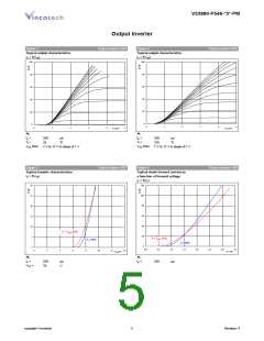
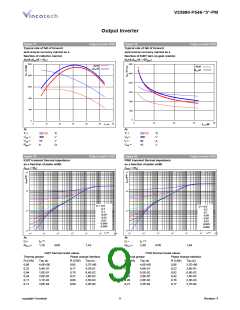
Figure 17
Output inverter FWD
Figure 18
Output inverter FWD
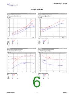
Typical rate of fall of forward
and reverse recovery current as a
function of collector current
dI0/dt,dIrec/dt = f(IC)
Typical rate of fall of forward
and reverse recovery current as a
function of IGBT turn on gate resistor
dI0/dt,dIrec/dt = f(Rgon
)
2000
2400
dI0/dt
dI0/dt
µ
µ
µ
µ
dIrec/dt
dIrec/dt
2000
1600
1200
800
1600
1200
800
400
0
400
0
0
20
40
60
80
0
10
20
30
40
50
60
I C (A)
R gon ( Ω )
At
At
Tj =
VCE
VGE
Tj =
°C
V
°C
V
A
V
25/125
300
15
25/125
=
=
VR =
300
30
IF =
V
Rgon
=
VGE =
8
ꢀ
15
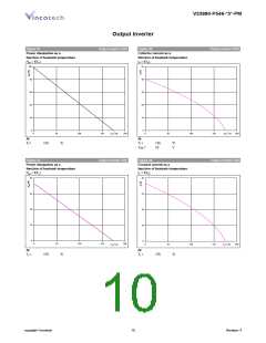
Figure 19
Output inverter IGBT
Figure 20
Output inverter FWD
IGBT transient thermal impedance
as a function of pulse width
ZthJH = f(tp)
FWD transient thermal impedance
as a function of pulse width
ZthJH = f(tp)
101
101
100
100
D = 0,5
0,2
D = 0,5
0,2
10-1
10-1
0,1
0,1
0,05
0,02
0,01
0,005
0.000
0,05
0,02
0,01
0,005
0.000
10-2
10-2
10-5
10-5
10-4
10-3
10-2
10-1
100
10110
10-4
10-3
10-2
10-1
100
10110
t p (s)
t p (s)
At
At
tp / T
1,76
tp / T
2,40
D =
D =
RthJH
=
RthJH =
K/W
1,43
K/W
1,94
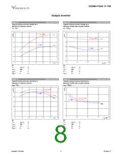
IGBT thermal model values
Phase change interface
FWD thermal model values
Thermal grease Phase change interface
Thermal grease
R (C/W)
0,06
Tau (s)
R (C/W)
0,05
Tau (s)
R (C/W)
0,07
Tau (s)
R (C/W)
0,06
Tau (s)
4,6E+00
5,4E-01
1,0E-01
2,0E-02
3,1E-03
3,0E-04
3,7E+00
4,3E-01
8,4E-02
1,6E-02
2,5E-03
2,4E-04
4,6E+00
4,8E-01
8,5E-02
2,0E-02
2,8E-03
3,3E-04
3,7E+00
3,9E-01
6,9E-02
1,6E-02
2,3E-03
2,7E-04
0,22
0,17
0,27
0,22
0,94
0,76
1,13
0,92
0,34
0,27
0,52
0,42
0,11
0,09
0,20
0,16
0,11
0,09
0,21
0,17
copyright Vincotech
9
Revision: 4

 VINCOTECH [ VINCOTECH ]