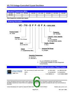
VC-710 Voltage Controlled Crystal Oscillator
Electrical Performance
Parameter
Symbol
fO
Min
120
3.135
Typical
155.52
3.3
Maximum
200
Units
MHz
V
Frequency
Supply Voltage
(+3.3 V)
VDD
3.465
Supply Current
IDD
50
<90
mA
Output Logic Levels
Output Logic High
Output Logic Low
+25 ºC
+25 ºC
VOH
VOL
Vcc -1.025
Vcc -1.810
Vcc -0.950
Vcc -1.700
Vcc -0.880
Vcc -1.620
V
V
Transition Times
Rise Time
Fall Time
tR
tF
0.5
0.5
1
1
ns
ns
Symmetry or Duty Cycle
SYM
45
50
0/70 or –40/85
0.3
55
%
°C
ps (rms)
ps (rms)
Operating temperature (ordering option)
Jitter (12 kHz– 20 MHz BW), 155.52 MHz
Jitter (50 kHz– 80 MHz BW), 155.52 MHz
0.5
Phase Noise, f0 = 155.52 MHz
10 Hz offset
-64
-95
dBc/Hz
dBc/Hz
dBc/Hz
dBc/Hz
dBc/Hz
dBc/Hz
dBc/Hz
100 Hz offset
1kHz offset
10 kHz offset
100 kHz offset
1 MHz offset
-123
-143
-146
-146
-146
10 MHz offset
Test Conditions for APR (+3.3V)
VC
0.3
3.0
V
Absolute Pull Range (APR)
APR
+ 50
ppm
Gain Transfer
Control Voltage Bandwidth (-3dB)
Package Size
Positive, 65
100
5.0 x 7.5 x 1.8
ppm/V
kHz
mm
BW
20
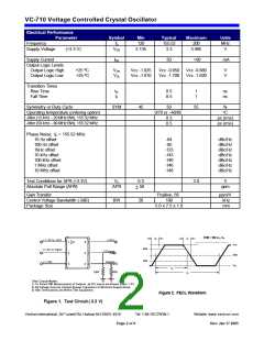
SYM = 100 x tA / tB
tR
tF
(-1.3V to +2V)
(+2V)
1
2
3
6
5
4
VOH
50%
VOL
80%
20%
>1.4V or Open
(-1.3V)
COutput
Output
tA
W
W
50
50
tB
Test Circuit Notes:
W
1) To Permit 50 Measurement of Outputs, all DC Inputs are Biased Down 1.3V.
2) All Voltage Sources Contain Bypass Capacitors to Minimize Supply Noise.
3) 50W Terminations are Within Test Equipment.
Figure 2. PECL Waveform
Figure 1. Test Circuit ( 3.3 V)
Vectron International, 267 Lowell Rd, Hudson NH 03051-4916
Tel: 1-88-VECTRON-1
Website: www.vectron.com
Page 2 of 6
Rev: Jan 17 2005

 VECTRON [ Vectron International, Inc ]