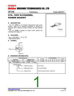
UF540
Preliminary
Power MOSFET
ABSOLUTE MAXIMUM RATINGS
PARAMETER
SYMBOL
VDSS
RATINGS
100
UNIT
V
Drain-Source Voltage (Note 2)
Gate-Source Voltage
VGSS
±20
V
TC=25°C
27
A
Continuous
ID
Drain Current
TC=100°C
17
A
Pulsed
Power Dissipation (TC=25°C)
Junction Temperature
Storage Temperature
IDM
PD
108
A
125
W
°C
°C
TJ
+150
-55~+150
TSTG
Notes: 1. Absolute maximum ratings are those values beyond which the device could be permanently damaged.
Absolute maximum ratings are stress ratings only and functional device operation is not implied.
2. TJ = +25~+150°C
THERMAL DATA
PARAMETER
SYMBOL
RATINGS
1.0
UNIT
°C/W
Junction to Case
θJC
ELECTRICAL CHARACTERISTICS (TC=25°C, unless otherwise noted)
PARAMETER
SYMBOL
TEST CONDITIONS
MIN TYP MAX UNIT
OFF CHARACTERISTICS
Drain-Source Breakdown Voltage
Drain-Source Leakage Current
BVDSS
IDSS
ID=250µA, VGS=0V
VDS=100V, VGS=0V
VGS=+20V, VDS=0V
100
V
250 µA
+500 nA
-500 nA
Forward
Reverse
Gate-Source Leakage Current
IGSS
VGS=-20V, VDS=0V
ON CHARACTERISTICS
Gate Threshold Voltage
VGS(TH)
RDS(ON)
VDS=VGS, ID=250µA
VGS=10V, ID=15A
2.0
4.0
V
Static Drain-Source On-State Resistance
DYNAMIC PARAMETERS
Input Capacitance
0.085
Ω
CISS
COSS
CRSS
1960
250
40
pF
pF
pF
Output Capacitance
VGS=0V, VDS=25V, f=1.0MHz
Reverse Transfer Capacitance
SWITCHING PARAMETERS
Turn-ON Delay Time
Rise Time
tD(ON)
tR
tD(OFF)
tF
11
35
39
35
71
14
21
ns
ns
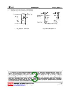
VDD=45V, ID=15A, VGS=10V,
RGEN=5.1Ω (Fig.1, 2)
Turn-OFF Delay Time
Fall-Time
ns
(Note 2)
ns
Total Gate Charge
QG
VDD=35V, ID=27A, VGS=10V,
nC
nC
nC
Gate to Source Charge
Gate to Drain Charge
QGS
QGD
SOURCE- DRAIN DIODE RATINGS AND CHARACTERISTICS
Drain-Source Diode Forward Voltage
Body Diode Reverse Recovery Time
Maximum Body-Diode Continuous Current
Maximum Body-Diode Pulsed Current
Notes: 1. Pulse width limited by TJ
VSD
trr
IS=27A, VGS=0V
2.0 2.5
300
V
ns
A
IS=4.0A, dIS/dt=25A/µs
IS
27
ISM
108
A
2. Switching time measurements performed on LEM TR-58 Test equipment
UNISONIC TECHNOLOGIES CO., LTD
2 of 3
QW-R502-715.a
www.unisonic.com.tw

 UTC [ Unisonic Technologies ]