UC3846
LINEAR INTEGRATED CIRCUIT
OPERATION DESCRIPTION(Cont.)
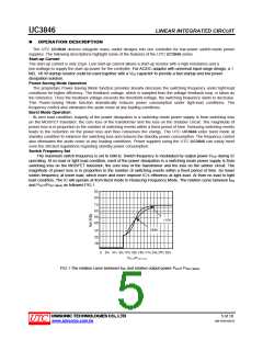
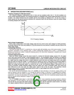
Frequency Hopping For EMI Improvement
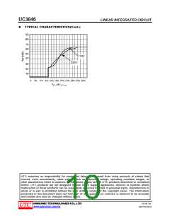
The Frequency hopping is implemented in the IC; there are two oscillators built-in the IC. The first oscillator is to
set the normal switching frequency; the switching frequency is modulated with a period signal generated by the 2nd
oscillator. The relation between the first oscillator and the 2nd oscillator as followed FIG.2. So the tone energy is
evenly spread out, the spread spectrum minimizes the conduction band EMI and therefore eases the system design
in meeting stringent EMI requirement.
FIG.2 Frequency Hopping
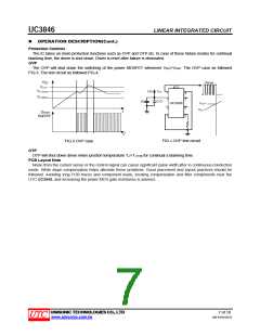
Built-in Slope Compensation
Built-in slope compensation circuit adds voltage ramp onto the current sense input voltage for PWM generation,
this greatly improves the close loop stability at CCM and prevents the sub-harmonic oscillation and thus reduces the
output ripple voltage.
Leading-Edge Blanking
Each time the power MOSFET is switched on, a turn-on spike will inevitably occur at the sense-resistor. To avoid
premature termination of the switching pulse, a 400ns leading-edge blanking time is built in. Conventional RC
filtering can therefore be omitted. During this blanking period, the current-limit comparator is disabled and it cannot
switch off the gate driver.
Constant Output Power Limit
When the SENSE voltage, across the sense resistor RS, reaches the threshold voltage, around 0.8V, the output
GATE drive will be turned off after a small propagation delay tD. This propagation delay will introduce an additional
current proportional to tD×VIN/Lp. Since the propagation delay is nearly constant regardless of the input line voltage
VIN. Higher input line voltage will result in a larger additional current and hence the output power limit is also higher
than that under low input line voltage. To compensate this variation for wide AC input range, the threshold voltage is
adjusted by the VIN current. Since VIN pin is connected to the rectified input line voltage through a resistor RVIN, a
higher line voltage will generate higher VIN current into the VIN pin. The threshold voltage is decreased if the VIN
current is increased. Smaller threshold voltage, forces the output GATE drive to terminate earlier, thus reduce the
total PWM turn-on time and make the output power equal to that of low line input. This proprietary internal
compensation ensures a constant output power limit for wide AC input voltage from 90VAC to 264VAC.
Under Voltage Lockout (UVLO)
The turn-on and turn-off thresholds of the UTC UC3846 are fixed internally at 14.2V/8.2V. During start-up, the
hold-up capacitor must be charged to 14.2V through the start-up resistor, so that the UTC UC3846 will be enabled.
The hold-up capacitor will continue to supply VDD until power can be delivered from the auxiliary winding of the main
transformer. VDD must not drop below 8.2V during this start-up process. This UVLO hysteresis window ensures that
hold-up capacitor will be adequate to supply VDD during start-up.
Gate Output
The UTC UC3846 output stage is a fast totem pole gate driver. Cross conduction has been avoided to minimize
heat dissipation, increase efficiency, and enhance reliability. A good tradeoff is achieved through dead time control.
The low idle loss and good EMI system design is easier to achieve with this dedicated control scheme. An internal
18V clamp is added for MOSFET gate protection at higher than expected VDD input.
UNISONIC TECHNOLOGIES CO., LTD
6 of 10
QW-R103-053.B
www.unisonic.com.tw

 UTC [ Unisonic Technologies ]