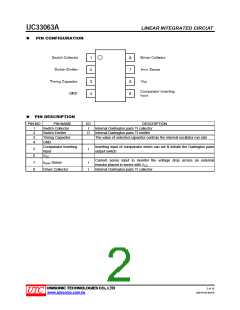
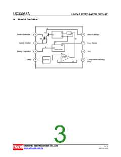
UC33063A
LINEAR INTEGRATED CIRCUIT
ABSOLUTE MAXIMUM RATINGS (Ta=25°C )
PARAMETER
SYMBOL
VCC
RATINGS
40
UNIT
V
Supply Voltage
Comparator Input Voltage Range
Switch Collector Voltage
Switch Emitter Voltage
VIN(COMP)
VC(SW)
VE(SW)
VCE(SW)
VC(DR)
ISW
-0.3 ~ +40
40
V
V
40
V
Switch Collector to Emitter Voltage
Driver Collector Voltage
Switch Current
40
V
40
V
1.5
A
DIP-8
1250
800
Power Dissipation (Ta=25°C)
PD
mW
SOP-8
Junction Temperature
Operating Temperature
Storage Temperature
TJ
+150
-40~ +90
-65 ~ +150
°C
°C
°C
TOPR
TSTG
Note: Absolute maximum ratings are those values beyond which the device could be permanently damaged.
Absolute maximum ratings are stress ratings only and functional device operation is not implied.
THERMAL DATA
PARAMETER
SYMBOL
RATINGS
100
UNIT
DIP-8
Junction to Ambient
θJA
°C/W
SOP-8
150
ELECTRICAL CHARACTERISTICS (VCC=5.0V, Ta=-40~+90°C, unless otherwise specified.)
PARAMETER
SYMBOL
TEST CONDITIONS
MIN TYP MAX UNIT
Oscillator
Charging Current
ICHG
IDISCHG
VOSC
K
VCC=5 to 40V, Ta=25°C
VCC=5 to 40V, Ta=25°C
Ta=25°C
V7=VCC, Ta=25°C
ICHG=IDISCHG, Ta=25°C
22
31
42
μA
Discharging Current
Oscillator Amplitude
Discharge to Charge Current Ratio
Current limit Sense Voltage
Output Switch
140 190 260 μA
0.5
6.1
V
5.2
7.5
VSENSE
250 300 350 mV
Saturation Voltage 1(Note)
Saturation Voltage 2(Note)
DC Current Gain(Note)
Collector Off State Current(Note)
Comparator
VCE(SAT)1 ISW=1.0A, VC(DRIVER)=VC(SW)
VCE(SAT)2 ISW=1.0A, VC(DRIVER)=50mA
0.95 1.3
0.45 0.7
180
V
V
GI (DC)
IC(OFF)
ISW=1.0A, VCE=5.0V, Ta=25°C
VCE=40.0V, Ta=25°C
50
0.01 100 μA
Threshold Voltage
VTHD
VTHD
II(BIAS)
1.21 1.24 1.29
V
Threshold Voltage Line Regulation
Input Bias Current
VCC=3 ~ 40V
VIN=0V
2.0
50
5.0 mV
400 nA
Total Device
V
CC=5~40V, CT=0.001
Supply Current
ICC
2.7
4.0 mA
V7=VCC, VC>VTHD, Pin2=GND
Note: Output switch tests are performed under pulsed conditions to minimize power dissipation.
UNISONIC TECHNOLOGIES CO., LTD
4 of 10
QW-R103-044.B
www.unisonic.com.tw

 UTC [ Unisonic Technologies ]