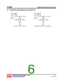
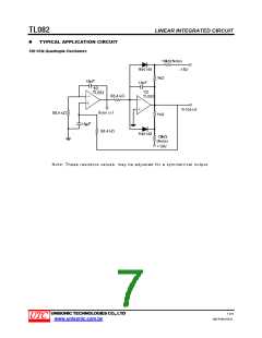
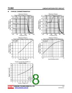
TL082
LINEAR INTEGRATED CIRCUIT
ABSOLUTE MAXIMUM RATING (Ta=25°C)
PARAMETER
SYMBOL
VCC
RATINGS
±18
UNIT
V
Supply Voltage (Note 2)
Input Voltage (Note 3)
VIN
±15
V
Differential Input Voltage (Note 4)
Power Dissipation
VID
±30
V
PD
680
mW
Output Short-Circuit Duration (Note 5)
Operating Temperature
Infinite
-20 ~ +85
-65 ~ +150
TOPR
TSTG
°C
°C
Storage Temperature Range
Note: 1. Absolute maximum ratings are those values beyond which the device could be permanently damaged.
Absolute maximum ratings are stress ratings only and functional device operation is not implied.
2. All voltage values, except differential voltage, are with respect to the zero reference level (ground) of the
supply voltages where the zero reference level is the midpoint between VCC- and VCC+.
3. The magnitude of the input voltage must never exceed the magnitude of the supply voltage or 15 volts,
whichever is less.
4. Differential voltages are at the non-inverting input terminal with respect to the inverting input terminal.
5. The output may be shorted to ground or to either supply. Temperature and/or supply voltages must be
limited to ensure that the dissipation rating is not exceeded.
THERMAL DATA
PARAMETER
SYMBOL
RATINGS
125
85
UNIT
°C/W
°C/W
°C/W
°C/W
°C/W
°C/W
SOP-8
DIP-8
Junction to Ambient
Junction to Case
θJA
TSSOP-8
SOP-8
DIP-8
120
40
θJC
41
TSSOP-8
37
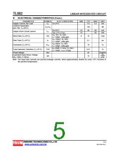
ELECTRICAL CHARACTERISTICS
( VCC=±15V, Ta=25°C, TMIN=0°C, TMAX=70°C , unless otherwise specified)
PARAMETER
Input Offset Voltage (RS=50Ω)
Input Offset Voltage Drift
Input Offset Current (Note)
SYMBOL
TEST CONDITIONS
Ta=25°C
MIN
TYP
MAX
10
UNIT
mV
3
VIO
TMIN ≤Ta ≤TMAX
13
DVIO
10
5
µV/°C
pA
nA
pA
nA
V
Ta=25°C
100
10
IIO
TMIN ≤Ta ≤TMAX
Ta=25°C
20
400
20
Input Bias Current (Note)
IIB
TMIN ≤Ta ≤TMAX
Input Common Mode Voltage Range
VICM
±11 -12~+15
Ta=25°C, RL=2kΩ,
Ta=25°C, RL=10kΩ
TMIN ≤Ta ≤TMAX, RL=2kΩ
TMIN ≤Ta≤ TMAX, RL=10kΩ
Ta=25°C
10
12
10
12
25
15
12
V
13.5
V
Output Voltage Swing
±VOPP
Avd
V
V
Large Signal Voltage Gain
(RL=2kΩ, VOUT=±10V)
200
4
V/mV
TMIN ≤Ta ≤TMAX
VIN=10mV, RL=2kΩ, CL=100pF,
f=100kHZ
Gain Bandwidth Product (Ta=25°C)
GBP
RI
2.5
MHz
Ω
Input Resistance
1012
86
Common Mode Rejection Ratio
(RS=50Ω)
Ta=25°C
70
70
70
70
CMR
dB
TMIN ≤Ta ≤TMAX
Ta=25°C
Supply Voltage Rejection Ratio
(RS=50Ω)
86
SVR
dB
TMIN ≤Ta ≤TMAX
UNISONIC TECHNOLOGIES CO., LTD
www.unisonic.com.tw
4 of 9
QW-R105-019,G

 UTC [ Unisonic Technologies ]