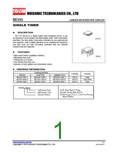
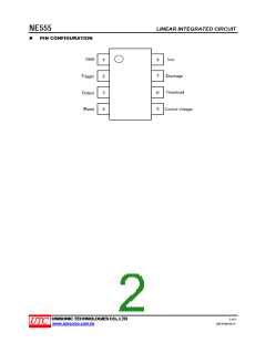
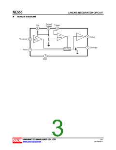
NE555
LINEAR INTEGRATED CIRCUIT
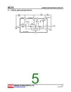
TYPICAL APPLICATION NOTES
The application circuit shows astable mode configuration.
Pin 6 (Threshold ) is tied to Pin 2 ( Trigger ) and Pin 4 ( reset ) is tied to VCC ( Pin 8 ). The external capacitor C1 of
Pin 6 and Pin 2 charges through RA, RB and dischages through RB only. In the internal circuit of UTC NE555 , one
input of the upper comparator is at voltage of 2/3Vcc(R1=R2=R3),another input is connected to Pin 6.As soon
as C1 is charging to higher than 2/3Vcc, transistor Q1 is turned ON and discharge C1 to collector voltage of
transistor Q1. Therefore, the flip-flop circuit is reset and output is low. One input of lower comparator is at voltage of
1/3Vcc, discharge transistor Q1 turn off and C1 charges through RA and RB. Therefore, the flip-flop circuit is set
output high.
That is, when C1 charges through RA and RB , output is high and when C1 discharge through RB ,output is low.
The charge time(output is high) t1 is 0.693(RA+RB) C1 and the discharge time (output is low) T2 is 0.693 RB*C1.
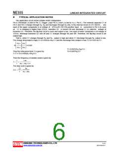
1
Vcc− Vcc
3
2
Vcc− Vcc
3
⎛
⎜
⎞
⎟
ln
=0.693
⎜
⎟
⎜
⎟
⎠
⎝
T1=0.693*(RA+RB)*C1
T2=0.693*RB*C1
Thus the total period time T is given by
T=T1+T2=0.693(RA+2RB)*C1.
Then the frequency of astable mode is given by
1
1.44
f =
=
T
(RA + 2RB) * C1
The duty cycle is given by
T2
RB
D.C. =
=
T
RA + 2RB
.
UNISONIC TECHNOLOGIES CO., LTD
6 of 8
www.unisonic.com.tw
QW-R106-001,F

 UTC [ Unisonic Technologies ]