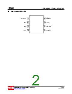
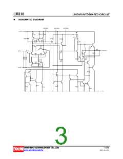
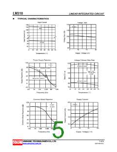
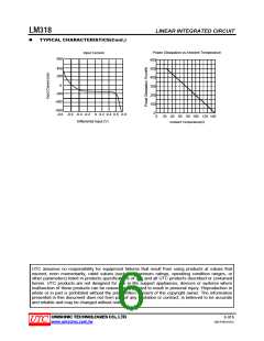
LM318
LINEAR INTEGRATED CIRCUIT
ABSOLUTE MAXIMUM RATINGS
PARAMETER
SYMBOL
VCC+
VCC-
RATINGS
+20
UNIT
V
Supply Voltage
Supply Voltage
-20
V
Input Voltage (Note 2)
VIN
±15
V
Differential Input Current (Note 3)
Power Dissipation
II(DIFF)
PD
±10
mA
mW
500
Output Short-Circuit Duration
Maximum Junction Temperature
Operating Temperature Range
Storage Temperature Range
Continuous
110
TJ
°C
°C
°C
TOPR
TSTG
0 ~ +70
-65 ~ +150
Note:1.Absolute maximum ratings are those values beyond which the device could be permanently damaged.
Absolute maximum ratings are stress ratings only and functional device operation is not implied.
2.For supply voltage less than ±15V, the absolute maximum input voltage is equal to the supply voltage.
3.The inputs are shunted with two opposite-facing base-emitter diodes for over voltage protection. Therefore,
excessive current flows if a differential input voltage in excess of 1V is applied between the inputs unless
some limiting resistance is used.
ELECTRICAL CHARACTERISTICS (±5V≤ VCC ≤±20V, 0°C≤TA≤+70°C, unless other specifics)
PARAMETER
SYMBOL
VIN
TEST CONDITION
VCC=±15V
MIN TYP
±11.5
MAX
UNIT
V
Input Voltage Range
Output Voltage Swing
VOUT
VCC =±15V, RL=2KΩ
TA=25°C
±12
±13
4
V
10
15
mV
mV
Input Offset Voltage
VI(OFF)
TA=25°C, VCC =±15V
25
20
200
V/mV
Large Signal Voltage Gain
GV
VOUT=±10V, RL≥2KΩ
Vcc =±15V, VOUT=±10V, RL≥2KΩ
V/mV
nA
TA=25°C
TA=25°C
30
200
300
500
750
10
Input Offset Current
Input Bias Current
II(OFF)
II(BIAS)
nA
150
nA
nA
Supply Current
ISS
RS
TA=25°C
TA=25°C
TA=25°C, VCC =±15V, Gv=1
TA=25°C, VCC =±15V
5
3
mA
MΩ
V/µs
MHz
dB
Input Resistance
0.5
50
Slew Rate
SR
70
15
100
80
Small Signal Bandwidth
Common Mode Rejection Ratio
Supply Voltage Rejection Ratio
SBW
CMRR
SVRR
70
65
dB
Note: These power supplies must be bypassed with 0.1µF(or larger) disc ceramic capacitor within an inch of the
device.
UNISONIC TECHNOLOGIES CO., LTD
4 of 6
QW-R105-016,C
www.unisonic.com.tw

 UTC [ Unisonic Technologies ]