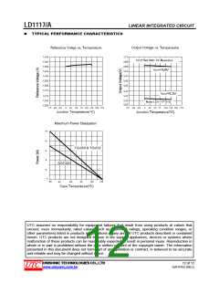
LD1117/A
LINEAR INTEGRATED CIRCUIT
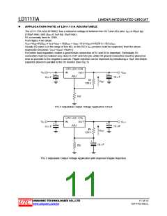
APPLICATION NOTE of LD1117/A ADJUSTABLE
The LD1117/A ADJUSTABLE has a reference voltage of between the OUT and ADJ pins. IADJ is 60μA typ.
(120μA max.) and ΔIADJ is 1μA typ. (5μA max.).
R1 is normally fixed to 120Ω.
From figure 4 we obtain:
VOUT=VREF+R2(IADJ + IR1)=VREF + R2(IADJ + VREF / R1)=VREF(1+R2/R1) + R2 x IADJ.
Usually R2 value is in the range of few KΩ, so the R2 X IADJ product could be neglected; then the above
expression becomes: VOUT=VREF(1+R2/R1)
For better load regulation, realize a good Kelvin connection of R1 and R2 is important. Particularly R1
connection must be realized very close to OUT and ADJ pin, while R2 ground connection must be placed as
near as possible to the negative Load pin. Ripple rejection can be improved by introducing a 10μF electrolytic
capacitor placed in parallel to the R2 resistor (See Fig. 5)
UTC LD1117/A
VIN
VOUT
IN
OUT
+
+
ADJ
10μF
10μF
R1
120Ω
VREF
R2
FIG.4 Adjustable Output Voltage Application Circuit
FIG.5 Adjustable Output Voltage Application with improved Ripple Rejection.
UNISONIC TECHNOLOGIES CO., LTD
11 of 12
QW-R102-006,Q
www.unisonic.com.tw

 UTC [ Unisonic Technologies ]