78DxxA
Linear Integrated Circuit
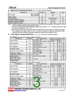
ꢀ ABSOLUATE MAXIUM RATINGS (Ta = 25℃,unless otherwise specified)
PARAMETER
SYMBOL
VIN
RATINGS
UNIT
V
VOUT =3.3~18V
OUT =20~24V
35
40
Input Voltage
V
Output Current
IOUT
PD
1
A
Power Dissipation
Internally Limited
-40 ~ +85
0~+125
-40 ~ +150
W
Operating Temperature Range
Operating Junction Temperature
Storage Temperature Range
TOPR
TJ
°C
°C
°C
TSTG
Note:1. Absolute maximum ratings are stress ratings only and functional device operation is not implied. The device
could be damaged beyond Absolute maximum ratings.
2. The device is guaranteed to meet performance specifications within 0℃~70℃ operating temperature range
and assured by design from –40℃~85℃.
3.The maximum steady state usable output current are dependent on input voltage, heat sinking, lead length
of the package and copper pattern of PCB. The data are showed as electrical characteristics table
represents pulse test conditions with junction temperatures specified at the initiation of test.
ꢀ
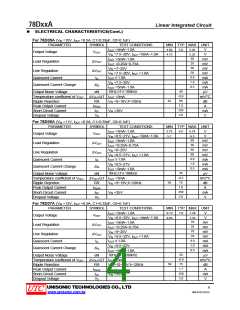
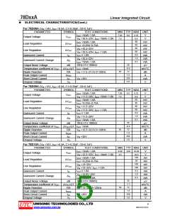
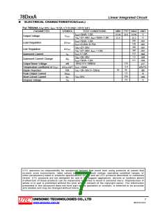
ELECTRICAL CHARACTERISTICS (TJ=25℃, PD≦15W, unless otherwise specified)
For 78D33A (VIN =5.8V, IOUT =0.5A, C1=0.33uF, C0=0.1uF)
PARAMETER
Output Voltage
SYMBOL
VOUT
TEST CONDITIONS
IOUT=5mA ~ 1.0A
MIN TYP MAX
3.168 3.30 3.432
UNIT
V
V
IN =5.8~18.3V, IOUT=5mA~1.0A 3.135
IOUT=5mA~1.0A
OUT=0.25A~0.75A
VIN =5.8~18.3V
IN =5.8~18.3V, IOUT=1.0A
OUT≦1.0A
3.465
33
V
mV
mV
mV
mV
mA
mA
mA
µV
Load Regulation
∆VOUT
I
17
33
Line Regulation
∆VOUT
IQ
V
I
33
Quiescent Current
8.0
1.0
0.5
VIN =5.8~18.3V
IOUT =5mA~1.0A
10Hz≦f≦100kHz
Quiescent Current Change
∆IQ
eN
Output Noise Voltage
55
-0.4
57
Temperature coefficient of VOUT ∆VOUT/∆T IOUT =5mA
Ripple Rejection
mV/°C
dB
RR
IPEAK
ISC
VIN =6.3~16.3V,f=120Hz
Peak Output Current
Short-Circuit Current
Dropout Voltage
1.8
250
2.0
A
VIN =35V
mA
V
VD
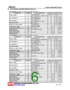
For 78D47A (VIN =9.7V, IOUT =0.5A, C1=0.33uF, C0=0.1uF)
PARAMETER
SYMBOL
TEST CONDITIONS
IOUT =5mA~1.0A
MIN TYP MAX UNIT
4.512 4.70 4.888
V
V
Output Voltage
VOUT
4.465
4.935
47
VIN=5.8~18.3V, IOUT=5mA~1.0A
IOUT=5mA~1.0A
mV
mV
mV
mV
mA
mA
mA
µV
Load Regulation
∆VOUT
24
47
I
OUT=0.25A~0.75A
VIN =5.8~18.3V
IN =5.8~18.3V, IOUT =1.0A
OUT≦1.0A
Line Regulation
∆VOUT
IQ
47
V
I
8.0
1.0
0.5
Quiescent Current
VIN =5.8~18.3V
IOUT =5mA~1.0A
10Hz≦f≦100kHz
Quiescent Current Change
∆IQ
eN
40
-0.6
80
Output Noise Voltage
Temperature coefficient of VOUT ∆VOUT/∆T IOUT =5mA
Ripple Rejection
mV/°C
dB
62
RR
IPEAK
ISC
VIN =6.3~16.3V,f=120Hz
1.8
250
2.0
Peak Output Current
Short-Circuit Current
Dropout Voltage
A
VIN =35V
mA
V
VD
UNISONIC TECHNOLOGIES CO., LTD
3
www.unisonic.com.tw
QW-R101-010,F

 UTC [ Unisonic Technologies ]