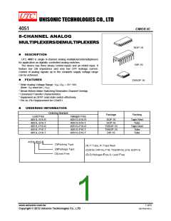
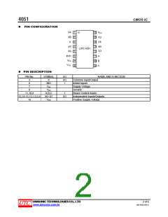
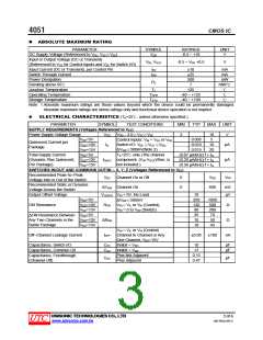
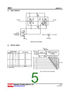
4051
CMOS IC
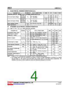
ELECTRICAL CHARACTERISTICS(Cont.)
PARAMETER
CONTROL INPUTS – INHIBIT A, B, C (Voltages Referenced to VSS
DD=5V
SYMBOL
TEST CONDITIONS
MIN
TYP
MAX
UNIT
V
)
V
2.25
4.50
4.0
1.5
3.0
R
ON= per spec,
Low Level Input Voltage
VDD=10V
VDD=15V
VIL
I
OFF = per spec
6.75
3.5
7
V
DD=5V
2.75
5.5
R
ON= per spec,
High Level Input Voltage
VDD=10V
VDD=15V
VIH
V
I
OFF = per spec
11
8.25
Input Leakage Current
Input Capacitance
ILEAK VIN= 0 or VDD, VDD=15V
CIN
±0.00001 ±0.1
5.0 7.5
µA
pF
DYNAMIC ELECTRICAL CHARACTERISTICS
(CL = 50pF, TA=25℃, VEE≦VSS, unless otherwise specified)
V
DD-VEE
VDC
5
PARAMETER
SYMBOL
TEST CONDITIONS
PLH, tPHL =(0.17 ns/pF)CL + 26.5ns
MIN TYP MAX UNIT
Propagation Delay Times
Switch Input to Switch
Output (RL = 10kΩ)
t
35
15
90
40
tPLH, tPHL
10
15
5
tPLH, tPHL =(0.08 ns/pF)CL + 11ns
tPLH, tPHL =(0.06 ns/pF)CL + 9ns
ns
ns
ns
12
30
(RL=10kΩ, VEE=VSS
)
350
170
140
360
160
120
0.07
700
340
280
720
320
240
t
t
PHZ, tPLZ
PZH, tPZL
Output “1” or “0” to High Impedance,
or High Impedance to “1” or “0” Level
Inhibit to Output
10
15
5
Control Input to Output
tPLH, tPHL
10
15
10
RL = 10kΩ, VEE = VSS
Total Harmonic Distortion
Bandwidth
THD
BW
RL = 10KΩ, f = 1 kHz, Vin = 5 VPP
RL = 1kΩ, VIN = 1/2 (VDD–VEE) p–p,
CL = 50pF, 20 Log (VOUT/VIN) = -3dB)
RL=1KΩ, VIN = 1/2 (VDD–VEE) p–p
IN = 4.5 MHz
RL = 1kΩ, VIN = 1/2 (VDD–VEE) p–p
IN = 3MHz
R1 = 1kΩ, RL = 10kΩ Control
TLH = tTHL = 20ns, Inhibit = VSS
%
10
10
10
10
17
-50
-50
75
MHz
Off Channel Feedthrough
Attenuation
dB
dB
f
Channel Separation
f
Crosstalk, Control Input to
Common O/I
mV
t
Note: 1. Data of “TYP” is intended as an indication of the IC’s potential performance.
2. For voltage drops across the switch(ΔVSW)>600mV (>300mV at high temperature), excessive VDD current
may be drawn, i.e. the current out of the switch may contain both VDD and switch input components. The
reliability of the device will be unaffected unless the Maximum Ratings are exceeded.
UNISONIC TECHNOLOGIES CO., LTD
4 of 6
QW-R502-054.C
www.unisonic.com.tw

 UTC [ Unisonic Technologies ]