Product specification
IRLML6401PbF
Electrical Characteristics @ TJ = 25°C (unless otherwise specified)
Parameter
Drain-to-Source Breakdown Voltage
Min. Typ. Max. Units
-12 ––– –––
Conditions
VGS = 0V, ID = -250µA
V(BR)DSS
V
∆V(BR)DSS/∆TJ Breakdown Voltage Temp. Coefficient
––– -0.007 ––– V/°C Reference to 25°C, ID = -1mA
––– ––– 0.050
––– 0.085
––– 0.125
-0.40 -0.55 -0.95
8.6 ––– –––
––– ––– -1.0
––– ––– -25
––– ––– -100
––– ––– 100
VGS = -4.5V, ID = -4.3A
VGS = -2.5V, ID = -2.5A
VGS = -1.8V, ID = -2.0A
VDS = VGS, ID = -250µA
VDS = -10V, ID = -4.3A
Ω
RDS(on)
Static Drain-to-Source On-Resistance
VGS(th)
gfs
Gate Threshold Voltage
V
S
Forward Transconductance
VDS = -12V, VGS = 0V
IDSS
Drain-to-Source Leakage Current
µA
nA
VDS = -9.6V, VGS = 0V, TJ = 55°C
Gate-to-Source Forward Leakage
Gate-to-Source Reverse Leakage
Total Gate Charge
VGS = -8.0V
IGSS
VGS = 8.0V
ID = -4.3A
Qg
––– 10
15
Qgs
Qgd
td(on)
tr
Gate-to-Source Charge
Gate-to-Drain ("Miller") Charge
Turn-On Delay Time
Rise Time
––– 1.4 2.1
––– 2.6 3.9
––– 11 –––
––– 32 –––
––– 250 –––
––– 210 –––
––– 830 –––
––– 180 –––
––– 125 –––
nC VDS = -10V
VGS = -5.0V
VDD = -6.0V
ns
ID = -1.0A
td(off)
tf
Turn-Off Delay Time
Fall Time
RD = 6.0Ω
RG = 89Ω
VGS = 0V
Ciss
Coss
Crss
Input Capacitance
Output Capacitance
pF VDS = -10V
ƒ = 1.0MHz
Reverse Transfer Capacitance
Source-Drain Ratings and Characteristics
Parameter
Continuous Source Current
(Body Diode)
Min. Typ. Max. Units
Conditions
D
S
IS
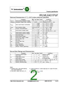
MOSFET symbol
showing the
-1.3
-34
––– –––
––– –––
A
G
ISM
Pulsed Source Current
(Body Diode)
integral reverse
p-n junction diode.
VSD
trr
Diode Forward Voltage
Reverse Recovery Time
Reverse RecoveryCharge
––– ––– -1.2
V
TJ = 25°C, IS = -1.3A, VGS = 0V
––– 22
––– 8.0
33
12
ns
TJ = 25°C, IF = -1.3A
Qrr
nC di/dt = -100A/µs
Notes:
Repetitive rating; pulse width limited by
max. junction temperature.
Surface mounted on 1" square single layer 1oz. copper FR4 board,
steady state.
Pulse width ≤ 300µs; duty cycle ≤ 2%.
Starting TJ = 25°C, L = 3.5mH
RG = 25Ω, IAS = -4.3A.
http://www.twtysemi.com
sales@twtysemi.com
4008-318-123
2 of 2

 TYSEMI [ TY Semiconductor Co., Ltd ]