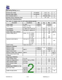
Thermal Performance
Condition
Thermal Resistance
Junction to Ambient
Package type
Typ
15
Unit
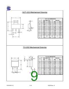
SOT-223
oC/W
SOP-8
20
TO-252
25
Note 1: Absolute Maximum Rating is limits beyond which damage to the device may occur. For guaranteed
specifications and test conditions see the Electrical Characteristics.
Note 2: The device is not guaranteed to operate outside its operating rating.
Note 3: Devices are ESD sensitive. Handling precautions recommended.
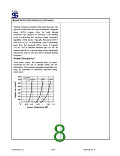
Note 4: The maximum allowable power dissipation is a function of the maximum junction temperature, Tj, the junction to
ambient thermal resistance, θja, and the ambient temperature, Ta. Exceeding the maximum allowable power
dissipation will cause excessive die temperature, and the regulator will go into thermal shutdown. The effective
value of θja can be reduced by using a heatsink, Pd(max) = (Tj(max) – Ta) / Θja.
Note 5: Dropout voltage is defined as the input to output differential at which the output voltage drops -1% below its
nominal value measured at 1V differential.
Note 6: Ground pin current is the regulator quiescent current. The total current drawn from the source is the sum of the
ground pin current and output load current, Iin = Ignd + Iout.
Note 7: Vref ≤ Vout ≤ (Vin – 1V), 2.25V ≤ Vin ≤ 16V, 10mA ≤ IL ≤ 1.0A.
Note 8: Output voltage temperature coefficient is ∆Vout (worse cast) / (Tj(max) - Tj(min)) where is Tj(max) +125 oC and
Tj(min) is 0 oC.
Note 9: For adjustable device and fiexed device with Vout > 2.25V.
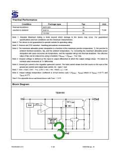
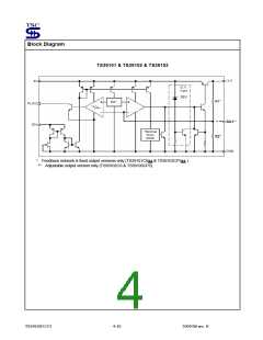
Block Diagram
TS39100
TS39100/1/2/3
3-10
2004/06 rev. E

 TSC [ TAIWAN SEMICONDUCTOR COMPANY, LTD ]