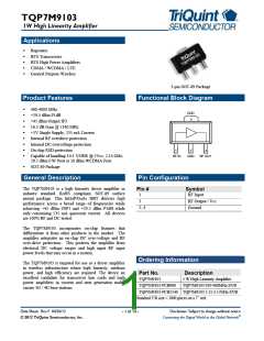
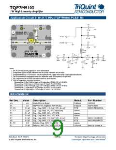
TQP7M9103
1W High Linearity Amplifier
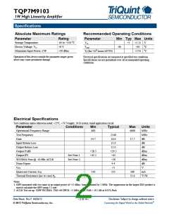
Specifications
Absolute Maximum Ratings
Recommended Operating Conditions
Parameter
Rating
Parameter
Vcc
Min Typ Max Units
Storage Temperature
Device Voltage, Vcc
Maximum Input Power, CW
-65 to +150 oC
+8 V
+5
+5.25
V
oC
Tcase
-40
+85
Tj (for>106 hours MTTF)
+170 oC
+30 dBm
Operation of this device outside the parameter ranges given
above may cause permanent damage.
Electrical specifications are measured at specified test conditions.
Specifications are not guaranteed over all recommended operating
conditions.
Electrical Specifications
Test conditions unless otherwise noted: +25ºC, +5V Vsupply, 50 Ω system, tuned application circuit
Parameter
Operational Frequency Range
Conditions
Min
400
Typical
Max
4000
Units
MHz
MHz
dB
Test Frequency
2140
16.6
12.0
15.0
+29.5
+45
+20
4.4
Gain
14.7
17.7
Input Return Loss
Output Return Loss
Output P1dB
dB
dB
+28.5
+42.5
dBm
dBm
dBm
dB
Output IP3
See Note 1.
See Note 2.
WCDMA Pout @ -50 dBc ACLR
Noise Figure
Vcc
+5
V
210
235
260
mA
oC/W
Quiescent Current, Icq
Thermal Resistance (jnc to case) θjc
35.6
Notes
1. OIP3 measured with two tones at an output power of +15 dBm / tone separated by 1 MHz. The suppression on the largest IM3 product is
used to calculate the OIP3 using 2:1 rule.
2. ACLR Test set-up: 3GPP WCDMA, TM1+64 DPCH, +5 MHz offset, PAR = 10.2 dB at 0.01% Prob.
Data Sheet: Rev F 04/26/12
Disclaimer: Subject to change without notice
Connecting the Digital World to the Global Network®
- 2 of 14 -
© 2012 TriQuint Semiconductor, Inc.

 TRIQUINT [ TRIQUINT SEMICONDUCTOR ]