88 / 102
TMC4670 Datasheet PRELIMINARY • IC Version V0.99 | Document Revision V0.91 • 2016-Nov-09
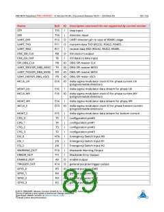
Name
Ball IO Description
ADC_BIP
B4
B7
O
O
O
I
output driving ADC LTC2351 BIP input
ADC_nSCS
ADC LTC2351 nSCS signal
ADC_SCK
B6
ADC LTC2351 SCK signal
ADC_MISO
ADC_MOSI
PWM_IDLE_H
PWM_IDLE_L
PWM_UX1_H
PWM_UX1_L
PWM_VX2_H
PWM_VX2_L
PWM_WY1_H
PWM_WY1_L
PWM_Y2_H
PWM_Y2_L
PWM_Z_OUT
PWM_C_OUT
BRAKE_OUT
DRV_ERR_IN
A6
from ADC LTC2351 SDO output
A7
O
I
reserved for ADC w/ SDI input
A11
B11
D16
D15
C16
D14
B16
C15
B15
C14
L15
L16
A13
A12
Idle Level of high side gate control signals
Idle Level of low side gate control signals
high side gate control output U (3-phase) resp. X1 (2-phase)
low side gate control output U (3-phase) resp. X1 (2-phase)
high side gate control output V (3-phase) resp. X2 (2-phase)
low side gate control output V (3-phase) resp. X2 (2-phase)
high side gate control output W (3-phase) resp. Y1 (2-phase)
low side gate control output W (3-phase) resp. Y1 (2-phase)
high side gate control output Y2 (2-phase only)
low side gate control output Y2 (2-phase only)
pulse, indicating start of PWM period (zero count)
pulse, indicating center of PWM period
I
O
O
O
O
O
O
O
O
O
O
O
I
brake chopper control signal
driver error input (from gate driver)
Table 8: Functional Pin Description
©2016 TRINAMIC Motion Control GmbH & Co. KG, Hamburg, Germany
Terms of delivery and rights to technical change reserved.
Download newest version at www.trinamic.com
Read entire documentation.

 TRINAMIC [ TRINAMIC MOTION CONTROL GMBH & CO. KG. ]