TMC2160 DATASHEET (Rev. 1.02 / 2018-NOV-19)
13
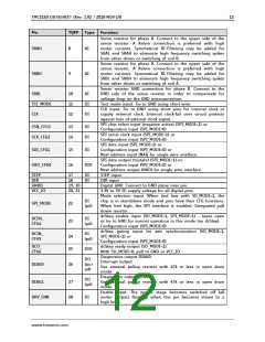
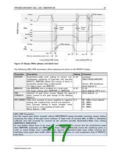
Pin
TQFP Type Function
5V supply input for digital circuitry within chip. Provide 100nF
or bigger capacitor to GND (GND plane) near pin. Shall be
supplied by 5VOUT. A 2.2 or 3.3 Ohm resistor is recommended
for decoupling noise from 5VOUT. When using an external
supply, make sure, that VCC comes up before or in parallel to
5VOUT or VCC_IO, whichever comes up later!
Charge pump capacitor output.
VCC
29
CPO
CPI
31
32
Charge pump capacitor input. Tie to CPO using 22nF, 100V
capacitor.
Motor supply voltage. Provide filtering capacity near pin with
short loop to GND plane. Must be tied to the positive bridge
supply voltage.
VS
33
VCP
CA2
HA2
BMA2
LA2
34
35
36
37
38
39
40
41
42
43
44
45
46
47
48
Charge pump voltage. Tie to VS using 100nF capacitor.
Bootstrap capacitor positive connection.
High side gate driver output.
Bridge Center and bootstrap capacitor negative connection.
Low side gate driver output.
Low side gate driver output.
Bridge Center and bootstrap capacitor negative connection.
High side gate driver output.
Bootstrap capacitor positive connection.
Bootstrap capacitor positive connection.
High side gate driver output.
Bridge Center and bootstrap capacitor negative connection.
Low side gate driver output.
Low side gate driver output.
Bridge Center and bootstrap capacitor negative connection.
Connect the exposed die pad to a GND plane. Provide as many
as possible vias for heat transfer to GND plane. Serves as GND
pin for the low side gate drivers. Ensure low loop inductivity
to sense resistor GND.
LA1
BMA1
HA1
CA1
CB2
HB2
BMB2
LB2
LB1
BMB1
Exposed die pad -
*(pd) denominates a pin with pulldown resistor
* All digital pins DI, DIO and DO use VCC_IO level and contain protection diodes to GND and VCC_IO
* All digital inputs DI and DIO have internal Schmitt-Triggers
www.trinamic.com

 TRINAMIC [ TRINAMIC MOTION CONTROL GMBH & CO. KG. ]