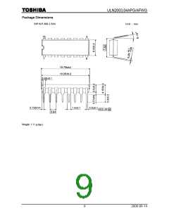
ULN2003,04APG/AFWG
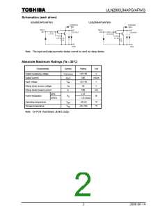
Schematics (each driver)
ULN2003APG/AFWG
ULN2004APG/AFWG
Note: The input and output parasitic diodes cannot be used as clamp diodes.
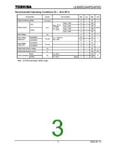
Absolute Maximum Ratings (Ta = 25°C)
Characteristic
Symbol
Rating
Unit
Output sustaining voltage
Output current
V
−0.5~50
500
V
mA/ch
V
CE (SUS)
I
OUT
Input voltage
V
−0.5~30
50
IN
Clamp diode reverse voltage
Clamp diode forward current
V
V
R
D
I
500
mA
F
APG
AFWG
1.47
Power dissipation
P
W
1.25 (Note)
−40~85
−55~150
Operating temperature
Storage temperature
T
opr
°C
°C
T
stg
Note: On PCB (Test Board: JEDEC 2s2p)
2
2006-06-14

 TOSHIBA [ TOSHIBA ]