欢迎访问ic37.com |
会员登录 免费注册
发布采购

TMP86P202MG 参数 Datasheet PDF下载

TMP86P202MG图片预览
型号: TMP86P202MG
PDF下载: 下载PDF文件 查看货源
内容描述: 8位微控制器 [8 Bit Microcontroller]
分类和应用: 微控制器
文件页数/大小: 108 页 / 1113 K
品牌: TOSHIBA [ TOSHIBA ]
 浏览型号TMP86P202MG的Datasheet PDF文件第1页浏览型号TMP86P202MG的Datasheet PDF文件第2页浏览型号TMP86P202MG的Datasheet PDF文件第3页浏览型号TMP86P202MG的Datasheet PDF文件第5页浏览型号TMP86P202MG的Datasheet PDF文件第6页浏览型号TMP86P202MG的Datasheet PDF文件第7页浏览型号TMP86P202MG的Datasheet PDF文件第8页浏览型号TMP86P202MG的Datasheet PDF文件第9页  
Table of Contents  
TMP86P202MG  
1.1 Features . . . . . . . . . . . . . . . . . . . . . . . . . . . . . . . . . . . . . . . . . . . . . . . . . . . . . . . . . 1  
1.2 Pin Assignment . . . . . . . . . . . . . . . . . . . . . . . . . . . . . . . . . . . . . . . . . . . . . . . . . . . . 3  
1.3 Block Diagram . . . . . . . . . . . . . . . . . . . . . . . . . . . . . . . . . . . . . . . . . . . . . . . . . . . . . 4  
1.4 Pin Names and Functions . . . . . . . . . . . . . . . . . . . . . . . . . . . . . . . . . . . . . . . . . . . . 5  
2. Operational Description  
2.1 CPU Core Functions . . . . . . . . . . . . . . . . . . . . . . . . . . . . . . . . . . . . . . . . . . . . . . . . 7  
2.1.1 Memory Address Map............................................................................................................................... 7  
2.1.2 Program Memory (OTP) ........................................................................................................................... 7  
2.1.3 Data Memory (RAM)................................................................................................................................. 7  
2.2 System Clock Controller . . . . . . . . . . . . . . . . . . . . . . . . . . . . . . . . . . . . . . . . . . . . . 8  
2.2.1 Clock Generator........................................................................................................................................ 8  
2.2.2 Timing Generator.................................................................................................................................... 10  
2.2.2.1 Configuration of timing generator  
2.2.2.2 Machine cycle  
2.2.3 Operation Mode Control Circuit .............................................................................................................. 11  
2.2.3.1 Single-clock mode  
2.2.3.2 STOP mode  
2.2.4 Operating Mode Control ......................................................................................................................... 14  
2.2.4.1 STOP mode  
2.2.4.2 IDLE1 mode  
2.2.4.3 IDLE0 mode (IDLE0)  
2.3 Reset Circuit . . . . . . . . . . . . . . . . . . . . . . . . . . . . . . . . . . . . . . . . . . . . . . . . . . . . . 24  
2.3.1 External Reset Input ............................................................................................................................... 24  
2.3.2 Address trap reset .................................................................................................................................. 25  
2.3.3 Watchdog timer reset.............................................................................................................................. 25  
2.3.4 System clock reset.................................................................................................................................. 25  
3. Interrupt Control Circuit  
3.1 Interrupt latches (IL15 to IL2) . . . . . . . . . . . . . . . . . . . . . . . . . . . . . . . . . . . . . . . . 27  
3.2 Interrupt enable register (EIR). . . . . . . . . . . . . . . . . . . . . . . . . . . . . . . . . . . . . . . . 28  
3.2.1 Interrupt master enable flag (IMF) .......................................................................................................... 28  
3.2.2 Individual interrupt enable flags (EF15 to EF4) ...................................................................................... 28  
Note 3: . . . . . . . . . . . . . . . . . . . . . . . . . . . . . . . . . . . . . . . . . . . . . . . . . . . . . . . . . . . . . 30  
3.3 Interrupt Sequence . . . . . . . . . . . . . . . . . . . . . . . . . . . . . . . . . . . . . . . . . . . . . . . . 30  
3.3.1 Interrupt acceptance processing is packaged as follows........................................................................ 30  
3.3.2 Saving/restoring general-purpose registers............................................................................................ 32  
3.3.2.1 Using PUSH and POP instructions  
3.3.2.2 Using data transfer instructions  
3.3.3 Interrupt return ........................................................................................................................................ 33  
3.4 Software Interrupt (INTSW). . . . . . . . . . . . . . . . . . . . . . . . . . . . . . . . . . . . . . . . . . 34  
3.4.1 Address error detection .......................................................................................................................... 34  
3.4.2 Debugging .............................................................................................................................................. 34  
3.5 Undefined Instruction Interrupt (INTUNDEF). . . . . . . . . . . . . . . . . . . . . . . . . . . . . 34  
i
3.6 Address Trap Interrupt (INTATRAP) . . . . . . . . . . . . . . . . . . . . . . . . . . . . . . . . . . . 34  
3.7 External Interrupts . . . . . . . . . . . . . . . . . . . . . . . . . . . . . . . . . . . . . . . . . . . . . . . . . 34  
4. Special Function Register (SFR)  
4.1 SFR . . . . . . . . . . . . . . . . . . . . . . . . . . . . . . . . . . . . . . . . . . . . . . . . . . . . . . . . . . . . 37  
5. I/O Ports  
5.1 P0 (P01 to P00) Port (High Current) . . . . . . . . . . . . . . . . . . . . . . . . . . . . . . . . . . . 40  
5.2 P1 (P12 to P10) Port . . . . . . . . . . . . . . . . . . . . . . . . . . . . . . . . . . . . . . . . . . . . . . . 41  
5.3 P2 (P20) Port. . . . . . . . . . . . . . . . . . . . . . . . . . . . . . . . . . . . . . . . . . . . . . . . . . . . . 42  
5.4 P3 (P37 to P30) Port . . . . . . . . . . . . . . . . . . . . . . . . . . . . . . . . . . . . . . . . . . . . . . . 43  
6. Watchdog Timer (WDT)  
6.1 Watchdog Timer Configuration . . . . . . . . . . . . . . . . . . . . . . . . . . . . . . . . . . . . . . . 45  
6.2 Watchdog Timer Control . . . . . . . . . . . . . . . . . . . . . . . . . . . . . . . . . . . . . . . . . . . . 46  
6.2.1 Malfunction Detection Methods Using the Watchdog Timer................................................................... 46  
6.2.2 Watchdog Timer Enable ......................................................................................................................... 47  
6.2.3 Watchdog Timer Disable ........................................................................................................................ 48  
6.2.4 Watchdog Timer Interrupt (INTWDT)...................................................................................................... 48  
6.2.5 Watchdog Timer Reset........................................................................................................................... 49  
6.3 Address Trap. . . . . . . . . . . . . . . . . . . . . . . . . . . . . . . . . . . . . . . . . . . . . . . . . . . . . 50  
6.3.1 Selection of Address Trap in Internal RAM (ATAS)................................................................................ 50  
6.3.2 Selection of Operation at Address Trap (ATOUT).................................................................................. 50  
6.3.3 Address Trap Interrupt (INTATRAP)....................................................................................................... 50  
6.3.4 Address Trap Reset................................................................................................................................ 51  
7. Time Base Timer (TBT)  
7.1 Time Base Timer . . . . . . . . . . . . . . . . . . . . . . . . . . . . . . . . . . . . . . . . . . . . . . . . . . 53  
7.1.1 Configuration .......................................................................................................................................... 53  
7.1.2 Control .................................................................................................................................................... 53  
7.1.3 Function.................................................................................................................................................. 54  
7.2 Divider Output (DVO) . . . . . . . . . . . . . . . . . . . . . . . . . . . . . . . . . . . . . . . . . . . . . . 55  
7.2.1 Configuration .......................................................................................................................................... 55  
7.2.2 Control .................................................................................................................................................... 55  
8. 8-Bit TimerCounter (TC3, TC4)  
8.1 Configuration . . . . . . . . . . . . . . . . . . . . . . . . . . . . . . . . . . . . . . . . . . . . . . . . . . . . . 57  
8.2 TimerCounter Control . . . . . . . . . . . . . . . . . . . . . . . . . . . . . . . . . . . . . . . . . . . . . . 58  
8.3 Function. . . . . . . . . . . . . . . . . . . . . . . . . . . . . . . . . . . . . . . . . . . . . . . . . . . . . . . . . 62  
8.3.1 8-Bit Timer Mode (TC3 and 4) ................................................................................................................ 62  
8.3.2 8-Bit Event Counter Mode (TC3, 4) ........................................................................................................ 63  
8.3.3 8-Bit Programmable Divider Output (PDO) Mode (TC3, 4)..................................................................... 63  
8.3.4 8-Bit Pulse Width Modulation (PWM) Output Mode (TC3, 4).................................................................. 65  
8.3.5 16-Bit Timer Mode (TC3 and 4) .............................................................................................................. 67  
8.3.6 16-Bit Event Counter Mode (TC3 and 4) ................................................................................................ 68  
8.3.7 16-Bit Pulse Width Modulation (PWM) Output Mode (TC3 and 4).......................................................... 68  
ii  
8.3.8 16-Bit Programmable Pulse Generate (PPG) Output Mode (TC3 and 4)............................................... 71  
9. 8-Bit AD Converter (ADC)  
9.1 Configuration . . . . . . . . . . . . . . . . . . . . . . . . . . . . . . . . . . . . . . . . . . . . . . . . . . . . . 73  
9.2 Control. . . . . . . . . . . . . . . . . . . . . . . . . . . . . . . . . . . . . . . . . . . . . . . . . . . . . . . . . . 74  
9.3 Function. . . . . . . . . . . . . . . . . . . . . . . . . . . . . . . . . . . . . . . . . . . . . . . . . . . . . . . . . 76  
9.3.1 AD Converter Operation ......................................................................................................................... 76  
9.3.2 AD Converter Operation ......................................................................................................................... 76  
9.3.3 STOP Mode during AD Conversion........................................................................................................ 77  
9.3.4 Analog Input Voltage and AD Conversion Result ................................................................................... 78  
9.4 Precautions about AD Converter. . . . . . . . . . . . . . . . . . . . . . . . . . . . . . . . . . . . . . 79  
9.4.1 Analog input pin voltage range ............................................................................................................... 79  
9.4.2 Analog input shared pins ........................................................................................................................ 79  
9.4.3 Noise countermeasure............................................................................................................................ 79  
10. OTP operation  
10.1 Operating mode. . . . . . . . . . . . . . . . . . . . . . . . . . . . . . . . . . . . . . . . . . . . . . . . . . 81  
10.1.1 MCU mode............................................................................................................................................ 81  
10.1.1.1 Program Memory  
10.1.1.2 Data Memory  
10.1.2 PROM mode ......................................................................................................................................... 81  
10.1.2.1 Programming Flowchart (High-speed program writing)  
10.1.2.2 Program Writing using a General-purpose PROM Programmer  
11. Input/Output Circuitry  
11.1 Control Pins. . . . . . . . . . . . . . . . . . . . . . . . . . . . . . . . . . . . . . . . . . . . . . . . . . . . . 87  
11.2 Input/Output Ports . . . . . . . . . . . . . . . . . . . . . . . . . . . . . . . . . . . . . . . . . . . . . . . . 88  
12. Electrical Characteristics  
12.1 Absolute Maximum Ratings. . . . . . . . . . . . . . . . . . . . . . . . . . . . . . . . . . . . . . . . . 89  
12.2 Operating Condition. . . . . . . . . . . . . . . . . . . . . . . . . . . . . . . . . . . . . . . . . . . . . . . 90  
12.3 DC Characteristics. . . . . . . . . . . . . . . . . . . . . . . . . . . . . . . . . . . . . . . . . . . . . . . . 91  
12.4 AD Conversion Characteristics . . . . . . . . . . . . . . . . . . . . . . . . . . . . . . . . . . . . . . 91  
12.5 AC Characteristics. . . . . . . . . . . . . . . . . . . . . . . . . . . . . . . . . . . . . . . . . . . . . . . . 92  
12.6 Recommended Oscillation Conditions. . . . . . . . . . . . . . . . . . . . . . . . . . . . . . . . . 92  
12.7 DC Characteristics, AC Characteristics (PROM mode). . . . . . . . . . . . . . . . . . . . 93  
12.7.1 Read operation in PROM mode............................................................................................................ 93  
12.7.2 Program operation (High-speed) (Topr = 25 ± 5°C) ............................................................................. 94  
12.8 Handling Precaution . . . . . . . . . . . . . . . . . . . . . . . . . . . . . . . . . . . . . . . . . . . . . . 95  
13. Package Dimensions  
This is a technical document that describes the operating functions and electrical  
iii  
specifications of the 8-bit microcontroller series TLCS-870/C (LSI).  
iv  
TMP86P202MG  
CMOS 8-Bit Microcontroller  
TMP86P202MG  
The TMP86P202MG is a single-chip 8-bit high-speed and high-functionality microcomputer incorporating 2048  
bytes of One-Time PROM.  
ROM  
Product No.  
RAM  
Package  
Emulation Chip  
TMP86C908XB  
(EPROM)  
2048  
bytes  
128  
TMP86P202MG  
SOP20-P-300-1.27  
bytes  
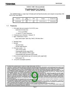
1.1 Features  
1. 8-bit single chip microcomputer TLCS-870/C series  
- Instruction execution time :  
0.50 µs (at 8 MHz)  
- 132 types & 731 basic instructions  
2. 11interrupt sources (External : 3 Internal : 8)  
3. Input / Output ports (14 pins)  
Large current output: 2pins (Typ. 20mA), LED direct drive  
4. Watchdog Timer  
5. Prescaler  
- Time base timer  
- Divider output function  
6. 8-bit timer counter : 2 ch  
- Timer, Event counter,  
- Programmable divider output (PDO),  
- Pulse width modulation (PWM) output,  
- Programmable pulse generation (PPG) modes  
7. 8-bit successive approximation type AD converter (with sample hold)  
Analog inputs: 4ch  
8. Low power consumption operation  
• The information contained herein is subject to change without notice. 021023_D  
• TOSHIBA is continually working to improve the quality and reliability of its products. Nevertheless, semiconductor devices in general can  
malfunction or fail due to their inherent electrical sensitivity and vulnerability to physical stress. It is the responsibility of the buyer, when  
utilizing TOSHIBA products, to comply with the standards of safety in making a safe design for the entire system, and to avoid situations  
in which a malfunction or failure of such TOSHIBA products could cause loss of human life, bodily injury or damage to property.  
In developing your designs, please ensure that TOSHIBA products are used within specified operating ranges as set forth in the most  
recent TOSHIBA products specifications. Also, please keep in mind the precautions and conditions set forth in the “Handling Guide for  
Semiconductor Devices,” or “TOSHIBA Semiconductor Reliability Handbook” etc. 021023_A  
• The TOSHIBA products listed in this document are intended for usage in general electronics applications (computer, personal equip-  
ment, office equipment, measuring equipment, industrial robotics, domestic appliances, etc.). These TOSHIBA products are neither  
intended nor warranted for usage in equipment that requires extraordinarily high quality and/or reliability or a malfunction or failure of  
which may cause loss of human life or bodily injury (“Unintended Usage”). Unintended Usage include atomic energy control instruments,  
airplane or spaceship instruments, transportation instruments, traffic signal instruments, combustion control instruments, medical instru-  
ments, all types of safety devices, etc. Unintended Usage of TOSHIBA products listed in this document shall be made at the customer's  
own risk. 021023_B  
• The products described in this document shall not be used or embedded to any downstream products of which manufacture, use and/or  
sale are prohibited under any applicable laws and regulations. 060106_Q  
• The information contained herein is presented only as a guide for the applications of our products. No responsibility is assumed by  
TOSHIBA for any infringements of patents or other rights of the third parties which may result from its use. No license is granted by impli-  
cation or otherwise under any patents or other rights of TOSHIBA or the third parties. 070122_C  
• The products described in this document are subject to foreign exchange and foreign trade control laws. 060925_E  
• For a discussion of how the reliability of microcontrollers can be predicted, please refer to Section 1.3 of the chapter entitled Quality and  
Reliability Assurance/Handling Precautions. 030619_S  
Page 1  
1.1 Features  
TMP86P202MG  
STOP mode: Oscillation stops. (Battery/Capacitor back-up.)  
IDLE0 mode: CPU stops, and only the Time-Based-Timer(TBT) on peripherals operate using high fre-  
quency clock. Release by falling edge of the source clock which is set by TBTCR<TBTCK>.  
IDLE1 mode: CPU stops and peripherals operate using high frequency clock. Release by interru-  
puts(CPU restarts).  
9. Operation voltage:  
3.3 V to 5.5 V at 8MHz  
Note: AD conversion characteristics are guaranteed with limited supply voltage range (4.5V to 5.5V).  
If supply voltage is less than 4.5V then AD conversion accuracy can not be guaranteed.  
Page 2  
TMP86P202MG  
1.2 Pin Assignment  
VSS  
XIN  
XOUT  
TEST  
1
2
3
4
5
6
7
8
20 P37 (AIN5)  
19  
18  
17  
P36 (AIN4)  
P35 (AIN3)  
P34 (AIN2)  
16 P33  
15 P32  
VDD  
P00  
P01  
RESET  
14  
13  
12  
11  
P31 (TC4/PDO4/PWM4/PPG4)  
P30 (TC3/PDO3/PWM3)  
P12 (DVO)  
(INT5/STOP) P20  
9
(INT0) P10 10  
P11 (INT1)  
Figure 1-1 Pin Assignment  
Page 3  
1.3 Block Diagram  
TMP86P202MG  
1.3 Block Diagram  
Figure 1-2 Block Diagram  
Page 4  
TMP86P202MG  
1.4 Pin Names and Functions  
The TMP86P202MG has MCU mode and PROM mode. Table 1-1 shows the pin functions in MCU mode. The  
PROM mode is explained later in a separate chapter.  
Table 1-1 Pin Names and Functions  
Pin Name  
Pin Number  
Input/Output  
Functions  
P01  
P00  
7
6
IO  
IO  
PORT01  
PORT00  
P12  
DVO  
IO  
O
PORT12  
12  
11  
10  
Divider Output  
P11  
IO  
I
PORT11  
INT1  
External interrupt 1 input  
P10  
INT0  
IO  
I
PORT10  
External interrupt 0 input  
P20  
IO  
PORT20  
STOP  
INT5  
9
I
I
STOP mode release signal input  
External interrupt 5 input  
P37  
IO  
I
PORT37  
20  
19  
18  
17  
AIN5  
AD converter analog input 5  
P36  
IO  
I
PORT36  
AIN4  
AD converter analog input 4  
P35  
IO  
I
PORT35  
AIN3  
AD converter analog input 3  
P34  
IO  
I
PORT34  
AIN2  
AD converter analog input 2  
P33  
P32  
16  
15  
IO  
IO  
PORT33  
PORT32  
P31  
TC4  
IO  
I
PORT31  
14  
13  
TC4 input  
PDO4/PWM4/PPG4  
O
PDO4/PWM4/PPG4 output  
P30  
IO  
I
PORT30  
TC3  
TC3 input  
PDO3/PWM3  
O
PDO3/PWM3 output  
XIN  
2
3
8
4
5
1
I
O
I
Resonator connecting pins for high-frequency clock  
XOUT  
RESET  
TEST  
VDD  
Resonator connecting pins for high-frequency clock  
Reset signal  
I
Test pin for out-going test. Normally, be fixed to low.  
I
+5V  
VSS  
I
0(GND)  
Page 5  
1.4 Pin Names and Functions  
TMP86P202MG  
Page 6  
TMP86P202MG  
2. Operational Description  
2.1 CPU Core Functions  
The CPU core consists of a CPU, a system clock controller, and an interrupt controller.  
This section provides a description of the CPU core, the program memory, the data memory, and the reset circuit.  
2.1.1 Memory Address Map  
The TMP86P202MG memory is composed OTP RAM, and SFR(Special function register). They are all  
mapped in 64-Kbyte address space. Figure 2-1 shows the TMP86P202MG memory address map.  
0000  
H
Special function register includes:  
I/O ports  
SFR:  
SFR  
64 bytes  
003F  
0040  
H
H
Peripheral control registers  
Peripheral status registers  
System control registers  
Program status word  
Random access memory includes:  
Data memory  
128  
bytes  
RAM  
RAM:  
OTP  
Stack  
00BF  
F800  
H
H
Program memory  
2048  
bytes  
OTP  
FFC0  
H
Vector table for vector call instructions  
(32 bytes)  
FFDF  
FFE0  
H
H
Vector table for interrupts  
(32 bytes)  
FFFF  
H
Figure 2-1 Memory Address Map  
2.1.2 Program Memory (OTP)  
The TMP86P202MG has a 2048 bytes (Address F800H to FFFFH) of program memory (OTP).  
2.1.3 Data Memory (RAM)  
The TMP86P202MG has 128 bytes (Address 0040H to 00BFH) of internal RAM. The internal RAM are  
located in the direct area; instructions with shorten operations are available against such an area.  
The data memory contents become unstable when the power supply is turned on; therefore, the data memory  
should be initialized by an initialization routine.  
Page 7  
2. Operational Description  
2.2 System Clock Controller  
TMP86P202MG  
Example :Clears RAM to “00H”. (TMP86P202MG)  
LD  
HL, 0040H  
A, H  
; Start address setup  
LD  
; Initial value (00H) setup  
LD  
BC, 007FH  
(HL), A  
HL  
SRAMCLR:  
LD  
INC  
DEC  
JRS  
BC  
F, SRAMCLR  
2.2 System Clock Controller  
The system clock controller consists of a clock generator, a timing generator, and a standby controller.  
Timing generator control register  
TBTCR  
Clock  
generator  
0036  
H
XIN  
fc  
High-frequency  
clock oscillator  
Timing  
generator  
Standby controller  
XOUT  
0038  
0039  
H
H
SYSCR1  
SYSCR2  
System control registers  
System clocks  
Clock generator control  
Figure 2-2 System Colck Control  
2.2.1 Clock Generator  
The clock generator generates the basic clock which provides the system clocks supplied to the CPU core  
and peripheral hardware.  
The high-frequency (fc) clock can easily be obtained by connecting a resonator between the XIN and XOUT  
pins . Clock input from an external oscillator is also possible. In this case, external clock is applied to XIN pin  
with XOUT pin not connected.  
Page 8  
TMP86P202MG  
High-frequency clock  
XOUT XIN  
XIN  
XOUT  
(Open)  
(a) Crystal/Ceramic  
resonator  
(b) External oscillator  
Figure 2-3 Examples of Resonator Connection  
Note:The function to monitor the basic clock directly at external is not provided for hardware, however, with dis-  
abling all interrupts and watchdog timers, the oscillation frequency can be adjusted by monitoring the pulse  
which the fixed frequency is outputted to the port by the program.  
The system to require the adjustment of the oscillation frequency should create the program for the adjust-  
ment in advance.  
Page 9  
2. Operational Description  
2.2 System Clock Controller  
TMP86P202MG  
2.2.2 Timing Generator  
The timing generator generates the various system clocks supplied to the CPU core and peripheral hardware  
from the basic clock (fc). The timing generator provides the following functions.  
1. Generation of main system clock  
2. Generation of divider output (DVO) pulses  
3. Generation of source clocks for time base timer  
4. Generation of source clocks for watchdog timer  
5. Generation of internal source clocks for timer/counters  
6. Generation of warm-up clocks for releasing STOP mode  
2.2.2.1 Configuration of timing generator  
The timing generator consists of a 2-stage prescaler, a 21-stage divider, a main system clock generator,  
and machine cycle counters.  
As reset and STOP mode started/canceled, the prescaler and the divider are cleared to “0”.  
fc  
Machine cycle counters  
Prescaler  
fc/4  
Divider  
Divider  
High-frequency  
clock fc  
1
2
1
2
3
4
5
6
7
8 9 10 11 12 13 14 15 16 17 18 19 20 21  
Warm-up  
controller  
Watchdog  
timer  
Timer counter, Time-base-timer, divider output, etc.  
Figure 2-4 Configuration of Timing Generator  
Page 10  
TMP86P202MG  
2.2.2.2 Machine cycle  
Instruction execution and peripheral hardware operation are synchronized with the main system clock.  
The minimum instruction execution unit is called an “machine cycle”. There are a total of 10 different  
types of instructions for the TLCS-870/C Series: Ranging from 1-cycle instructions which require one  
machine cycle for execution to 10-cycle instructions which require 10 machine cycles for execution. A  
machine cycle consists of 4 states (S0 to S3), and each state consists of one main system clock.  
1/fc [s]  
Main system clock  
State  
S0  
S1  
S2  
S3  
S0  
S1  
S2  
S3  
Machine cycle  
Figure 2-5 Machine Cycle  
2.2.3 Operation Mode Control Circuit  
The operation mode control circuit starts and stops the oscillation circuit for the high-frequency clock. There  
are two operating modes: Single clock mode and STOP mode. These modes are controlled by the system con-  
trol registers (SYSCR1 and SYSCR2). Figure 2-6 shows the operating mode transition diagram.  
2.2.3.1 Single-clock mode  
The oscillation circuit for the high-frequency clock is used. The main-system clock is obtained from the  
high-frequency clock. In the single-clock mode, the machine cycle time is 4/fc [s].  
(1) NORMAL1 mode  
In this mode, both the CPU core and on-chip peripherals operate using the high-frequency clock.  
The TMP86P202MG is placed in this mode after reset.  
(2) IDLE1 mode  
In this mode, the internal oscillation circuit remains active. The CPU and the watchdog timer are  
halted; however on-chip peripherals remain active (Operate using the high-frequency clock).  
IDLE1 mode is started by SYSCR2<IDLE> = "1", and IDLE1 mode is released to NORMAL1  
mode by an interrupt request from the on-chip peripherals or external interrupt inputs. When the IMF  
(Interrupt master enable flag) is “1” (Interrupt enable), the execution will resume with the acceptance  
of the interrupt, and the operation will return to normal after the interrupt service is completed. When  
the IMF is “0” (Interrupt disable), the execution will resume with the instruction which follows the  
IDLE1 mode start instruction.  
(3) IDLE0 mode  
In this mode, all the circuit, except oscillator and the timer-base-timer, stops operation.  
This mode is enabled by SYSCR2<TGHALT> = "1".  
Page 11  
2. Operational Description  
2.2 System Clock Controller  
TMP86P202MG  
When IDLE0 mode starts, the CPU stops and the timing generator stops feeding the clock to the  
peripheral circuits other than TBT. Then, upon detecting the falling edge of the source clock selected  
with TBTCR<TBTCK>, the timing generator starts feeding the clock to all peripheral circuits.  
When returned from IDLE0 mode, the CPU restarts operating, entering NORMAL1 mode back  
again. IDLE0 mode is entered and returned regardless of how TBTCR<TBTEN> is set. When IMF =  
“1”, EF6 (TBT interrupt individual enable flag) = “1”, and TBTCR<TBTEN> = “1”, interrupt pro-  
cessing is performed. When IDLE0 mode is entered while TBTCR<TBTEN> = “1”, the INTTBT  
interrupt latch is set after returning to NORMAL1 mode.  
2.2.3.2 STOP mode  
In this mode, the internal oscillation circuit is turned off, causing all system operations to be halted. The  
internal status immediately prior to the halt is held with a lowest power consumption during STOP mode.  
STOP mode is started by the system control register 1 (SYSCR1), and STOP mode is released by a  
inputting (Either level-sensitive or edge-sensitive can be programmably selected) to the STOP pin. After  
the warm-up period is completed, the execution resumes with the instruction which follows the STOP  
mode start instruction.  
IDLE0  
RESET  
STOP  
Reset release  
mode  
SYSCR2<TGHALT> = "1"  
SYSCR2<IDLE> = "1"  
Note 1  
SYSCR1<STOP> = "1"  
IDLE1  
mode  
NORMAL1  
mode  
Interrupt  
STOP pin input  
Note 1: The mode is released by falling edge of TBTCR<TBTCK> setting.  
Figure 2-6 Operating Mode Transition Diagram  
Table 2-1 Operating Mode and Conditions  
Oscillator  
Other  
Machine Cycle  
Time  
Operating Mode  
CPU Core  
TBT  
High  
Peripherals  
Frequency  
RESET  
NORMAL1  
Reset  
Reset  
Reset  
Operate  
Oscillation  
Stop  
Operate  
4/fc [s]  
Single clock IDLE1  
IDLE0  
Operate  
Halt  
Halt  
Halt  
STOP  
Page 12  
TMP86P202MG  
System Control Register 1  
SYSCR1  
(0038H)  
7
6
5
0
4
3
2
1
0
STOP  
RELM  
OUTEN  
WUT  
(Initial value: 0000 00**)  
0: CPU core and peripherals remain active  
STOP  
STOP mode start  
R/W  
1: CPU core and peripherals are halted (Start STOP mode)  
Release method for STOP  
mode  
0: Edge-sensitive release  
1: Level-sensitive release  
RELM  
R/W  
R/W  
0: High impedance  
1: Output kept  
OUTEN  
Port output during STOP mode  
Return to NORMAL mode  
16  
00  
01  
10  
11  
3 x 2 /fc  
16  
Warm-up time at releasing  
STOP mode  
WUT  
R/W  
2
/fc  
14  
3 x 2 /fc  
14  
2
/fc  
Note 1: When STOP mode is released with RESET pin input, a return is made to NORMAL1.  
Note 2: fc: High-frequency clock [Hz], *; Don’t care  
Note 3: Bits 1 and 0 in SYSCR1 are read as undefined data when a read instruction is executed.  
Note 4: As the hardware becomes STOP mode under OUTEN = “0”, input value is fixed to “0”; therefore it may cause external  
interrupt request on account of falling edge.  
Note 5: Port P20 is used as STOP pin. Therefore, when stop mode is started, OUTEN does not affect to P20, and P20 becomes  
High-Z mode.  
Note 6: Always set bit5 in SYSCR1 to "0".  
Note 7: The warmig-up time should be set correctly for using oscillator.  
System Control Register 2  
7
6
5
4
3
2
1
0
SYSCR2  
(0039H)  
XEN  
"0"  
"0"  
IDLE  
TGHALT  
(Initial value: 1000 *0**)  
0: Turn off oscillation  
1: Turn on oscillation  
XEN  
High-frequency oscillator control  
R/W  
R/W  
CPU and watchdog timer control 0: CPU and watchdog timer remain active  
IDLE  
(IDLE1 mode)  
1: CPU and watchdog timer are stopped (Start IDLE1 mode)  
0: Feeding clock to all peripherals from TG  
(Start IDLE0 mode)  
TGHALT  
TG control (IDLE0 mode)  
Note 1: When SYSCR2<XEN> is cleard to "0", the device is reset.  
Note 2: *: Don’t care, TG: Timing generator, *; Don’t care  
Note 3: Bits 3, 1 and 0 in SYSCR2 are always read as undefined value.  
Note 4: Do not set IDLE and TGHALT to “1” simultaneously.  
Note 5: Because returning from IDLE0 to NORMAL1 is executed by the asynchronous internal clock, the period of IDLE0 mode  
might be shorter than the period setting by TBTCR<TBTCK>.  
Note 6: When IDLE1 mode is released, IDLE is automatically cleared to “0”.  
Note 7: When IDLE0 mode is released, TGHALT is automatically cleared to “0”.  
Note 8: Always clear bit6 and 5 in SYSCR2 to "0".  
Note 9: Before setting TGHALT to “1”, be sure to stop peripherals. If peripherals are not stopped, the interrupt latch of peripherals  
may be set after IDLE0 mode is released.  
Page 13  
2. Operational Description  
2.2 System Clock Controller  
TMP86P202MG  
2.2.4 Operating Mode Control  
2.2.4.1 STOP mode  
STOP mode is controlled by the system control register 1, the STOP pin input.  
The STOP pin is also used both as a port P20 and an INT5 (external interrupt input 5) pin. STOP mode is  
started by setting SYSCR1<STOP> to “1”. During STOP mode, the following status is maintained.  
1. Oscillations are turned off, and all internal operations are halted.  
2. The data memory, registers, the program status word and port output latches are all held in the  
status in effect before STOP mode was entered.  
3. The prescaler and the divider of the timing generator are cleared to “0”.  
4. The program counter holds the address 2 ahead of the instruction (e.g., [SET (SYSCR1).7])  
which started STOP mode.  
STOP mode includes a level-sensitive mode and an edge-sensitive mode, either of which can be  
selected with the SYSCR1<RELM>.  
Note 1: During STOP period (from start of STOP mode to end of warm up), due to changes in the external  
interrupt pin signal, interrupt latches may be set to “1” and interrupts may be accepted immediately  
after STOP mode is released. Before starting STOP mode, therefore, disable interrupts. Also, before  
enabling interrupts after STOP mode is released, clear unnecessary interrupt latches.  
(1) Level-sensitive release mode (RELM = “1”)  
In this mode, STOP mode is released by setting the STOP pin high. This mode is used for capacitor  
backup when the main power supply is cut off and long term battery backup.  
Even if an instruction for starting STOP mode is executed while STOP pin input is high, STOP  
mode does not start but instead the warm-up sequence starts immediately. Thus, to start STOP mode  
in the level-sensitive release mode, it is necessary for the program to first confirm that the STOP pin  
input is low. The following two methods can be used for confirmation.  
1. Testing a port.  
2. Using an external interrupt input INT5 (INT5 is a falling edge-sensitive input).  
Example 1 :Starting STOP mode from NORMAL mode by testing a port P20.  
LD  
(SYSCR1), 01010000B  
(P2PRD). 0  
; Sets up the level-sensitive release mode  
; Wait until the STOP pin input goes low level  
SSTOPH:  
TEST  
JRS  
DI  
F, SSTOPH  
; IMF 0  
SET  
(SYSCR1). 7  
; Starts STOP mode  
Example 2 :Starting STOP mode from NORMAL mode with an INT5 interrupt.  
PINT5:  
TEST  
JRS  
LD  
(P2PRD). 0  
; To reject noise, STOP mode does not start if  
port P20 is at high  
F, SINT5  
(SYSCR1), 01010000B  
; Sets up the level-sensitive release mode.  
; IMF 0  
DI  
SET  
RETI  
(SYSCR1). 7  
; Starts STOP mode  
SINT5:  
Page 14  
TMP86P202MG  
VIH  
STOP pin  
XOUT pin  
STOP  
operation  
NORMAL  
operation  
NORMAL  
operation  
Warm up  
Confirm by program that the  
STOP pin input is low and start  
STOP mode.  
STOP mode is released by the hardware.  
Always released if the STOP  
pin input is high.  
Figure 2-7 Level-sensitive Release Mode  
Note 1: Even if the STOP pin input is low after warm-up start, the STOP mode is not restarted.  
Note 2: In this case of changing to the level-sensitive mode from the edge-sensitive mode, the release  
mode is not switched until a rising edge of the STOP pin input is detected.  
(2) Edge-sensitive release mode (RELM = “0”)  
In this mode, STOP mode is released by a rising edge of the STOP pin input. This is used in appli-  
cations where a relatively short program is executed repeatedly at periodic intervals. This periodic  
signal (for example, a clock from a low-power consumption oscillator) is input to the STOP pin. In  
the edge-sensitive release mode, STOP mode is started even when the STOP pin input is high level.  
Example :Starting STOP mode from NORMAL mode  
DI  
; IMF 0  
LD  
(SYSCR1), 10010000B  
; Starts after specified to the edge-sensitive release mode  
VIH  
STOP pin  
XOUT pin  
NORMAL  
operation  
STOP  
operation  
STOP  
Warm up  
operation  
NORMAL  
operation  
STOP mode started  
by the program.  
STOP mode is released by the hardware at the rising  
edge of STOP pin input.  
Figure 2-8 Edge-sensitive Release Mode  
STOP mode is released by the following sequence.  
1. The high-frequency clock oscillator is turned on.  
2. A warm-up period is inserted to allow oscillation time to stabilize. During warm up, all  
internal operations remain halted. Four different warm-up times can be selected with the  
SYSCR1<WUT> in accordance with the resonator characteristics.  
3. When the warm-up time has elapsed, normal operation resumes with the instruction follow-  
ing the STOP mode start instruction.  
Page 15  
2. Operational Description  
2.2 System Clock Controller  
TMP86P202MG  
Note 1: When the STOP mode is released, the start is made after the prescaler and the divider of the  
timing generator are cleared to "0".  
Note 2: STOP mode can also be released by inputting low level on the RESET pin, which immediately  
performs the normal reset operation.  
Note 3: When STOP mode is released with a low hold voltage, the following cautions must be observed.  
The power supply voltage must be at the operating voltage level before releasing STOP mode.  
The RESET pin input must also be “H” level, rising together with the power supply voltage. In this  
case, if an external time constant circuit has been connected, the RESET pin input voltage will  
increase at a slower pace than the power supply voltage. At this time, there is a danger that a  
reset may occur if input voltage level of the RESET pin drops below the non-inverting high-level  
input voltage (Hysteresis input).  
Table 2-2 Warm-up Time Example (at fc = 8.0 MHz)  
WUT  
Warm-up Time [ms]  
00  
01  
10  
11  
24.576  
8.192  
6.144  
2.048  
Note 1: The warm-up time is obtained by dividing the basic clock by the divider. Therefore, the warm-up  
time may include a certain amount of error if there is any fluctuation of the oscillation frequency  
when STOP mode is released. Thus, the warm-up time must be considered as an approximate  
value.  
Page 16  
TMP86P202MG  
Figure 2-9 STOP Mode Start/Release  
Page 17  
2. Operational Description  
2.2 System Clock Controller  
TMP86P202MG  
2.2.4.2 IDLE1 mode  
IDLE1 mode is controlled by the system control register 2 (SYSCR2) and maskable interrupts. The fol-  
lowing status is maintained during this mode.  
1. Operation of the CPU and watchdog timer (WDT) is halted. On-chip peripherals continue to  
operate.  
2. The data memory, CPU registers, program status word and port output latches are all held in the  
status in effect before this mode were entered.  
3. The program counter holds the address 2 ahead of the instruction which starts this mode.  
Starting IDLE1 mode  
by instruction  
CPU and WDT are halted  
Yes  
Reset  
Reset input  
No  
No  
Interrupt request  
Yes  
“0”  
IMF  
“1” (Interrupt release mode)  
Interrupt processing  
Normal  
release mode  
Execution of the instruc-  
tion which follows the  
IDLE1 mode start  
instruction  
Figure 2-10 IDLE1 Mode  
Page 18  
TMP86P202MG  
• Start the IDLE1 mode  
After IMF is set to "0", set the individual interrupt enable flag (EF) which releases IDLE1  
mode. To start IDLE1 mode, set SYSCR2<IDLE> to “1”.  
Release the IDLE1 mode  
IDLE1 mode includes a normal release mode and an interrupt release mode. These modes are  
selected by interrupt master enable flag (IMF). After releasing IDLE1 mode, the  
SYSCR2<IDLE> is automatically cleared to “0” and the operation mode is returned to the  
mode preceding IDLE1 mode.  
IDLE1 mode can also be released by inputting low level on the RESET pin. After releasing  
reset, the operation mode is started from NORMAL1 mode.  
(1) Normal release mode (IMF = “0”)  
IDLE1 mode is released by any interrupt source enabled by the individual interrupt enable flag  
(EF). After the interrupt is generated, the program operation is resumed from the instruction follow-  
ing the IDLE1 mode starts instruction. Normally, the interrupt latches (IL) of the interrupt source  
used for releasing must be cleared to “0” by load instructions.  
(2) Interrupt release mode (IMF = “1”)  
IDLE1 mode are released by any interrupt source enabled with the individual interrupt enable flag  
(EF) and the interrupt processing is started. After the interrupt is processed, the program operation is  
resumed from the instruction following the instruction, which starts IDLE1 mode.  
Note: When a watchdog timer interrupts is generated immediately before IDLE1 mode are started, the  
watchdog timer interrupt will be processed but IDLE1 mode will not be started.  
Page 19  
2. Operational Description  
2.2 System Clock Controller  
TMP86P202MG  
Figure 2-11 IDLE1 Mode Start/Release  
Page 20  
TMP86P202MG  
2.2.4.3 IDLE0 mode (IDLE0)  
IDLE0 mode is controlled by the system control register 2 (SYSCR2) and the time base timer control  
register (TBTCR). The following status is maintained during IDLE0 mode.  
1. Timing generator stops feeding clock to peripherals except TBT.  
2. The data memory, CPU registers, program status word and port output latches are all held in the  
status in effect before IDLE0 mode was entered.  
3. The program counter holds the address 2 ahead of the instruction which starts IDLE0 mode.  
Note: Before starting IDLE0 mode, be sure to stop (Disable) peripherals.  
Stopping peripherals  
by instruction  
Starting IDLE0 mode by  
instruction  
CPU and WDT are halted  
Yes  
Reset input  
No  
Reset  
TBT  
source clock  
falling  
No  
No  
No  
No  
edge  
Yes  
TBTCR<TBTEN>  
= "1"  
Yes  
TBT interrupt  
enable  
Yes  
(Normal release mode)  
IMF = "1"  
Yes (Interrupt release mode)  
Interrupt processing  
Execution of the instruction  
which follows the IDLE0  
mode start instruction  
Figure 2-12 IDLE0 Mode  
Page 21  
2. Operational Description  
2.2 System Clock Controller  
TMP86P202MG  
Start the IDLE0 mode  
Stop (Disable) peripherals such as a timer counter.  
To start IDLE0 mode, set SYSCR2<TGHALT> to “1”.  
Release the IDLE0 mode  
IDLE0 mode include a normal release mode and an interrupt release mode.  
This mode is selected by interrupt master flag (IMF), the individual interrupt enable flag of  
TBT and TBTCR<TBTEN>.  
After releasing IDLE0 mode, the SYSCR2<TGHALT> is automatically cleared to “0” and  
the operation mode is returned to the mode preceding IDLE0 mode. Before starting the IDLE  
mode, when the TBTCR<TBTEN> is set to “1”, INTTBT interrupt latch is set to “1”.  
IDLE0 mode can also be released by inputting low level on the RESET pin. After releasing  
reset, the operation mode is started from NORMAL1 mode.  
Note: IDLE0 mode start/release without reference to TBTCR<TBTEN> setting.  
(1) Normal release mode (IMFEF6TBTCR<TBTEN> = “0”)  
IDLE0 mode are released by the source clock falling edge, which is setting by the  
TBTCR<TBTCK>. After the falling edge is detected, the program operation is resumed from the  
instruction following the IDLE0 mode start instruction. Before starting the IDLE mode, when the  
TBTCR<TBTEN> is set to “1”, INTTBT interrupt latch is set to “1”.  
(2) Interrupt release mode (IMFEF6TBTCR<TBTEN> = “1”)  
IDLE0 mode are released by the source clock falling edge, which is setting by the  
TBTCR<TBTCK> and INTTBT interrupt processing is started.  
Note 1: Because returning from IDLE0 to NORMAL1 is executed by the asynchronous internal clock,  
the period of IDLE0 mode might be the shorter than the period setting by TBTCR<TBTCK>.  
Note 2: When a watchdog timer interrupt is generated immediately before IDLE0 mode is started, the  
watchdog timer interrupt will be processed but IDLE0 mode will not be started.  
Page 22  
TMP86P202MG  
Figure 2-13 IDLE0 Mode Start/Release  
Page 23  
2. Operational Description  
2.3 Reset Circuit  
TMP86P202MG  
2.3 Reset Circuit  
The TMP86P202MG has four types of reset generation procedures: An external reset input, an address trap reset, a  
watchdog timer reset and a system clock reset. Of these reset, the address trap reset, the watchdog timer and the sys-  
tem clock reset are a malfunction reset. When the malfunction reset request is detected, reset occurs during the max-  
imum 24/fc[s].  
The malfunction reset circuit such as watchdog timer reset, address trap reset and system clock reset is not initial-  
ized when power is turned on. Therefore, reset may occur during maximum 24/fc[s] (3.0µs at 8.0 MHz) when power  
is turned on.  
Table 1-3 shows on-chip hardware initialization by reset action.  
Table 2-3 Initializing Internal Status by Reset Action  
On-chip Hardware  
Program counter  
Initial Value  
(FFFEH)  
On-chip Hardware  
Prescaler and divider of timing generator  
Watchdog timer  
Initial Value  
(PC)  
(SP)  
Stack pointer  
Not initialized  
0
General-purpose registers  
Not initialized  
(W, A, B, C, D, E, H, L, IX, IY)  
Jump status flag  
Zero flag  
(JF)  
(ZF)  
(CF)  
(HF)  
(SF)  
(VF)  
(IMF)  
(EF)  
(IL)  
Not initialized  
Not initialized  
Not initialized  
Not initialized  
Not initialized  
Not initialized  
0
Enable  
Carry flag  
Half carry flag  
Output latches of I/O ports  
Refer to I/O port circuitry  
Sign flag  
Overflow flag  
Interrupt master enable flag  
Interrupt individual enable flags  
Interrupt latches  
0
Refer to each of control  
register  
Control registers  
RAM  
0
Not initialized  
2.3.1 External Reset Input  
The RESET pin contains a Schmitt trigger (Hysteresis) with an internal pull-up resistor.  
When the RESET pin is held at “L” level for at least 3 machine cycles (12/fc [s]) with the power supply volt-  
age within the operating voltage range and oscillation stable, a reset is applied and the internal state is initial-  
ized.  
When the RESET pin input goes high, the reset operation is released and the program execution starts at the  
vector address stored at addresses FFFEH to FFFFH.  
VDD  
Internal reset  
RESET  
Watchdog timer reset  
Address trap reset  
System clock reset  
Malfunction  
reset output  
circuit  
Figure 2-14 Reset Circuit  
Page 24  
TMP86P202MG  
2.3.2 Address trap reset  
If the CPU should start looping for some cause such as noise and an attempt be made to fetch an instruction  
from the on-chip RAM (when WDTCR1<ATAS> is set to “1”) or the SFR area, address trap reset will be gen-  
erated. The reset time is maximum 24/fc[s] (3.0µs at 8.0 MHz).  
Note:The operating mode under address trapped is alternative of reset or interrupt. The address trap area is alter-  
native.  
Instruction  
execution  
Reset release  
16/fc [s]  
Instruction at address r  
JP a  
Address trap is occurred  
Maximum 24/fc [s]  
Internal reset  
4/fc to 12/fc [s]  
Note 1: Address “a” is in the SFR or on-chip RAM (WDTCR1<ATAS> = “1”) space.  
Note 2: During reset release, reset vector “r” is read out, and an instruction at address “r” is fetched and decoded.  
Figure 2-15 Address Trap Reset  
2.3.3 Watchdog timer reset  
Refer to 2.4 “Watchdog Timer”.  
2.3.4 System clock reset  
If the condition as follows is detected, the system clock reset occurs automatically to prevent dead lock of the  
CPU. (The oscillation is continued without stopping.)  
- In case of clearing SYSCR2<XEN> to 0.  
The reset time is maximum 24/fc (3.0 µs at 8.0 MHz).  
Page 25  
2. Operational Description  
2.3 Reset Circuit  
TMP86P202MG  
Page 26  
TMP86P202MG  
3. Interrupt Control Circuit  
The TMP86P202MG has a total of 11 interrupt sources excluding reset. Interrupts can be nested with priorities.  
Four of the internal interrupt sources are non-maskable while the rest are maskable.  
Interrupt sources are provided with interrupt latches (IL), which hold interrupt requests, and independent vectors.  
The interrupt latch is set to “1” by the generation of its interrupt request which requests the CPU to accept its inter-  
rupts. Interrupts are enabled or disabled by software using the interrupt master enable flag (IMF) and interrupt enable  
flag (EF). If more than one interrupts are generated simultaneously, interrupts are accepted in order which is domi-  
nated by hardware. However, there are no prioritized interrupt factors among non-maskable interrupts.  
Interrupt  
Latch  
Vector  
Interrupt Factors  
Enable Condition  
Non-maskable  
Priority  
Address  
Internal/External  
Internal  
(Reset)  
FFFE  
FFFC  
1
2
INTSWI (Software interrupt)  
Non-maskable  
Non-maskable  
INTUNDEF (Executed the undefined instruction  
interrupt)  
Internal  
FFFC  
2
Internal  
Internal  
External  
External  
Internal  
-
INTATRAP (Address trap interrupt)  
Non-maskable  
Non-maskable  
IMF• EF4 = 1, INT0EN = 1  
IMF• EF5 = 1  
IL2  
IL3  
FFFA  
FFF8  
FFF6  
FFF4  
FFF2  
FFF0  
FFEE  
FFEC  
FFEA  
FFE8  
FFE6  
FFE4  
FFE2  
FFE0  
2
2
INTWDT (Watchdog timer interrupt)  
INT0  
IL4  
5
INT1  
IL5  
6
INTTBT  
Reserved  
Reserved  
Reserved  
INTTC3  
INTTC4  
INTADC  
Reserved  
Reserved  
INT5  
IMF• EF6 = 1  
IL6  
7
IMF• EF7 = 1  
IL7  
8
-
IMF• EF8 = 1  
IL8  
9
-
IMF• EF9 = 1  
IL9  
10  
11  
12  
13  
14  
15  
16  
Internal  
Internal  
Internal  
-
IMF• EF10 = 1  
IMF• EF11 = 1  
IMF• EF12 = 1  
IMF• EF13 = 1  
IMF• EF14 = 1  
IMF• EF15 = 1  
IL10  
IL11  
IL12  
IL13  
IL14  
IL15  
-
External  
Note 1: To use the address trap interrupt (INTATRAP), clear WDTCR1<ATOUT> to “0” (It is set for the “reset request” after reset is  
cancelled). For details, see “Address Trap”.  
Note 2: To use the watchdog timer interrupt (INTWDT), clear WDTCR1<WDTOUT> to "0" (It is set for the "Reset request" after  
reset is released). For details, see "Watchdog Timer".  
3.1 Interrupt latches (IL15 to IL2)  
An interrupt latch is provided for each interrupt source, except for a software interrupt and an executed the unde-  
fined instruction interrupt. When interrupt request is generated, the latch is set to “1”, and the CPU is requested to  
accept the interrupt if its interrupt is enabled. The interrupt latch is cleared to "0" immediately after accepting inter-  
rupt. All interrupt latches are initialized to “0” during reset.  
The interrupt latches are located on address 003CH and 003DH in SFR area. Each latch can be cleared to "0" indi-  
vidually by instruction. However, IL2 and IL3 should not be cleared to "0" by software. For clearing the interrupt  
latch, load instruction should be used and then IL2 and IL3 should be set to "1". If the read-modify-write instructions  
such as bit manipulation or operation instructions are used, interrupt request would be cleared inadequately if inter-  
rupt is requested while such instructions are executed.  
Interrupt latches are not set to “1” by an instruction.  
Since interrupt latches can be read, the status for interrupt requests can be monitored by software.  
Note: In main program, before manipulating the interrupt enable flag (EF) or the interrupt latch (IL), be sure to clear IMF to  
"0" (Disable interrupt by DI instruction). Then set IMF newly again as required after operating on the EF or IL  
(Enable interrupt by EI instruction)  
In interrupt service routine, because the IMF becomes "0" automatically, clearing IMF need not execute normally on  
Page 27  
3. Interrupt Control Circuit  
3.2 Interrupt enable register (EIR)  
TMP86P202MG  
interrupt service routine. However, if using multiple interrupt on interrupt service routine, manipulating EF or IL  
should be executed before setting IMF="1".  
Example 1 :Clears interrupt latches  
DI  
; IMF 0  
LDW  
EI  
(ILL), 1110001110111111B  
; IL12 to IL10 , IL6 0  
; IMF 1  
Example 2 :Reads interrupt latchess  
LD  
WA, (ILL)  
; W ILH, A ILL  
Example 3 :Tests interrupt latches  
TEST  
JR  
(ILL). 6  
; if IL6 = 1 then jump  
F, SSET  
3.2 Interrupt enable register (EIR)  
The interrupt enable register (EIR) enables and disables the acceptance of interrupts, except for the non-maskable  
interrupts (Software interrupt, undefined instruction interrupt, address trap interrupt and watchdog interrupt). Non-  
maskable interrupt is accepted regardless of the contents of the EIR.  
The EIR consists of an interrupt master enable flag (IMF) and the individual interrupt enable flags (EF). These  
registers are located on address 003AH and 003BH in SFR area, and they can be read and written by an instructions  
(Including read-modify-write instructions such as bit manipulation or operation instructions).  
3.2.1 Interrupt master enable flag (IMF)  
The interrupt enable register (IMF) enables and disables the acceptance of the whole maskable interrupt.  
While IMF = “0”, all maskable interrupts are not accepted regardless of the status on each individual interrupt  
enable flag (EF). By setting IMF to “1”, the interrupt becomes acceptable if the individuals are enabled. When  
an interrupt is accepted, IMF is cleared to “0” after the latest status on IMF is stacked. Thus the maskable inter-  
rupts which follow are disabled. By executing return interrupt instruction [RETI/RETN], the stacked data,  
which was the status before interrupt acceptance, is loaded on IMF again.  
The IMF is located on bit0 in EIRL (Address: 003AH in SFR), and can be read and written by an instruction.  
The IMF is normally set and cleared by [EI] and [DI] instruction respectively. During reset, the IMF is initial-  
ized to “0”.  
3.2.2 Individual interrupt enable flags (EF15 to EF4)  
Each of these flags enables and disables the acceptance of its maskable interrupt. Setting the corresponding  
bit of an individual interrupt enable flag to “1” enables acceptance of its interrupt, and setting the bit to “0” dis-  
ables acceptance. During reset, all the individual interrupt enable flags (EF15 to EF4) are initialized to “0” and  
all maskable interrupts are not accepted until they are set to “1”.  
Note:In main program, before manipulating the interrupt enable flag (EF) or the interrupt latch (IL), be sure to clear  
IMF to "0" (Disable interrupt by DI instruction). Then set IMF newly again as required after operating on the EF  
or IL (Enable interrupt by EI instruction)  
In interrupt service routine, because the IMF becomes "0" automatically, clearing IMF need not execute nor-  
mally on interrupt service routine. However, if using multiple interrupt on interrupt service routine, manipulat-  
ing EF or IL should be executed before setting IMF="1".  
Page 28  
TMP86P202MG  
Example 1 :Enables interrupts individually and sets IMF  
DI  
; IMF 0  
LDW  
:
(EIRL), 1110100000100000B  
; EF15 to EF13, EF11, EF5 1  
Note: IMF should not be set.  
:
EI  
; IMF 1  
Example 2 :C compiler description example  
unsigned int _io (3AH) EIRL;  
/* 3AH shows EIRL address */  
_DI();  
EIRL = 10100000B;  
:
_EI();  
Page 29  
3. Interrupt Control Circuit  
3.3 Interrupt Sequence  
TMP86P202MG  
Interrupt Latches  
(Initial value: 0**000** *00000**)  
15  
IL15  
14  
13  
12  
11  
10  
9
8
7
6
5
4
3
2
1
0
ILH,ILL  
(003DH, 003CH)  
IL12  
IL11  
IL10  
IL6  
IL5  
IL4  
IL3  
IL2  
ILH (003DH)  
ILL (003CH)  
at WR  
at RD  
IL15 to IL2  
Interrupt latches  
R/W  
0: No interrupt request  
1: Interrupt request  
0: Clears the interrupt request  
1: (Interrupt latch is not set.)  
Note 1: To clear any one of bits IL6 to IL4, be sure to write "1" into IL2 and IL3.  
Note 2: In main program, before manipulating the interrupt enable flag (EF) or the interrupt latch (IL), be sure to clear IMF to "0"  
(Disable interrupt by DI instruction). Then set IMF newly again as required after operating on the EF or IL (Enable interrupt  
by EI instruction)  
In interrupt service routine, because the IMF becomes "0" automatically, clearing IMF need not execute normally on inter-  
rupt service routine. However, if using multiple interrupt on interrupt service routine, manipulating EF or IL should be exe-  
cuted before setting IMF="1".  
Note 3: Do not clear IL with read-modify-write instructions such as bit operations.  
Interrupt Enable Registers  
(Initial value: 0**000** *000***0)  
15  
14  
13  
12  
11  
10  
9
8
7
6
5
4
3
2
1
0
EIRH,EIRL  
(003BH, 003AH)  
EF15  
EF12 EF11 EF10  
EIRH (003BH)  
EF6  
EF5  
EF4  
IMF  
EIRL (003AH)  
Individual-interrupt enable flag  
(Specified for each bit)  
0: Disables the acceptance of each maskable interrupt.  
1: Enables the acceptance of each maskable interrupt.  
EF15 to EF4  
IMF  
R/W  
0: Disables the acceptance of all maskable interrupts  
1: Enables the acceptance of all maskable interrupts  
Interrupt master enable flag  
Note 1: *: Don’t care  
Note 2: Do not set IMF and the interrupt enable flag (EF15 to EF4) to “1” at the same time.  
Note 3: In main program, before manipulating the interrupt enable flag (EF) or the interrupt latch (IL), be sure to clear IMF to "0"  
(Disable interrupt by DI instruction). Then set IMF newly again as required after operating on the EF or IL (Enable interrupt  
by EI instruction)  
In interrupt service routine, because the IMF becomes "0" automatically, clearing IMF need not execute normally on inter-  
rupt service routine. However, if using multiple interrupt on interrupt service routine, manipulating EF or IL should be exe-  
cuted before setting IMF="1".  
3.3 Interrupt Sequence  
An interrupt request, which raised interrupt latch, is held, until interrupt is accepted or interrupt latch is cleared to  
“0” by resetting or an instruction. Interrupt acceptance sequence requires 8 machine cycles (4.0 µs @8.0 MHz) after  
the completion of the current instruction. The interrupt service task terminates upon execution of an interrupt return  
instruction [RETI] (for maskable interrupts) or [RETN] (for non-maskable interrupts). Figure 3-1 shows the timing  
chart of interrupt acceptance processing.  
3.3.1 Interrupt acceptance processing is packaged as follows.  
a. The interrupt master enable flag (IMF) is cleared to “0” in order to disable the acceptance of any fol-  
lowing interrupt.  
b. The interrupt latch (IL) for the interrupt source accepted is cleared to “0”.  
c. The contents of the program counter (PC) and the program status word, including the interrupt master  
enable flag (IMF), are saved (Pushed) on the stack in sequence of PSW + IMF, PCH, PCL. Mean-  
while, the stack pointer (SP) is decremented by 3.  
Page 30  
TMP86P202MG  
d. The entry address (Interrupt vector) of the corresponding interrupt service program, loaded on the vec-  
tor table, is transferred to the program counter.  
e. The instruction stored at the entry address of the interrupt service program is executed.  
Note:When the contents of PSW are saved on the stack, the contents of IMF are also saved.  
Interrupt service task  
1-machine cycle  
Interrupt  
request  
Interrupt  
latch (IL)  
IMF  
Execute  
instruction  
Execute  
instruction  
Execute  
instruction  
Execute RETI instruction  
Interrupt acceptance  
PC  
a
a + 1  
b
b + 1 b + 2 b + 3  
c + 1  
c + 2  
a
a 1  
a
a + 1 a + 2  
SP  
n
n
n 1 n 2  
n - 3  
n 2 n 1  
Note 1: a: Return address entry address, b: Entry address, c: Address which RETI instruction is stored  
Note 2: On condition that interrupt is enabled, it takes 38/fc [s] at maximum (If the interrupt latch is set at the first machine cycle on  
10 cycle instruction) to start interrupt acceptance processing since its interrupt latch is set.  
Figure 3-1 Timing Chart of Interrupt Acceptance/Return Interrupt Instruction  
Example: Correspondence between vector table address for INTTBT and the entry address of the interrupt  
service program  
Vector table address  
Entry address  
Interrupt  
service  
program  
FFF2H  
FFF3H  
03H  
D2H  
D203H  
D204H  
0FH  
06H  
Vector  
Figure 3-2 Vector table address, Entry address  
A maskable interrupt is not accepted until the IMF is set to “1” even if the maskable interrupt higher than the  
level of current servicing interrupt is requested.  
In order to utilize nested interrupt service, the IMF is set to “1” in the interrupt service program. In this case,  
acceptable interrupt sources are selectively enabled by the individual interrupt enable flags.  
To avoid overloaded nesting, clear the individual interrupt enable flag whose interrupt is currently serviced,  
before setting IMF to “1”. As for non-maskable interrupt, keep interrupt service shorten compared with length  
between interrupt requests; otherwise the status cannot be recovered as non-maskable interrupt would simply  
nested.  
Page 31  
3. Interrupt Control Circuit  
3.3 Interrupt Sequence  
TMP86P202MG  
3.3.2 Saving/restoring general-purpose registers  
During interrupt acceptance processing, the program counter (PC) and the program status word (PSW,  
includes IMF) are automatically saved on the stack, but the accumulator and others are not. These registers are  
saved by software if necessary. When multiple interrupt services are nested, it is also necessary to avoid using  
the same data memory area for saving registers. The following methods are used to save/restore the general-  
purpose registers.  
3.3.2.1 Using PUSH and POP instructions  
If only a specific register is saved or interrupts of the same source are nested, general-purpose registers  
can be saved/restored using the PUSH/POP instructions.  
Example :Save/store register using PUSH and POP instructions  
PINTxx:  
PUSH  
WA  
; Save WA register  
(interrupt processing)  
POP  
RETI  
WA  
; Restore WA register  
; RETURN  
Address  
(Example)  
SP  
b-5  
b-4  
b-3  
b-2  
b-1  
b
A
SP  
SP  
W
PCL  
PCH  
PSW  
PCL  
PCH  
PSW  
PCL  
PCH  
PSW  
SP  
At acceptance of  
an interrupt  
At execution of  
PUSH instruction  
At execution of  
POP instruction  
At execution of  
RETI instruction  
Figure 3-3 Save/store register using PUSH and POP instructions  
3.3.2.2 Using data transfer instructions  
To save only a specific register without nested interrupts, data transfer instructions are available.  
Example :Save/store register using data transfer instructions  
PINTxx:  
LD  
(GSAVA), A  
; Save A register  
(interrupt processing)  
LD  
A, (GSAVA)  
; Restore A register  
; RETURN  
RETI  
Page 32  
TMP86P202MG  
Main task  
Interrupt  
service task  
Interrupt  
acceptance  
Saving  
registers  
Restoring  
registers  
Interrupt return  
Saving/Restoring general-purpose registers using PUSH/POP data transfer instruction  
Figure 3-4 Saving/Restoring General-purpose Registers under Interrupt Processing  
3.3.3 Interrupt return  
Interrupt return instructions [RETI]/[RETN] perform as follows.  
[RETI]/[RETN] Interrupt Return  
1. Program counter (PC) and program status word  
(PSW, includes IMF) are restored from the stack.  
2. Stack pointer (SP) is incremented by 3.  
As for address trap interrupt (INTATRAP), it is required to alter stacked data for program counter (PC) to  
restarting address, during interrupt service program.  
Note:If [RETN] is executed with the above data unaltered, the program returns to the address trap area and  
INTATRAP occurs again.When interrupt acceptance processing has completed, stacked data for PCL and  
PCH are located on address (SP + 1) and (SP + 2) respectively.  
Example 1 :Returning from address trap interrupt (INTATRAP) service program  
PINTxx:  
POP  
LD  
WA  
; Recover SP by 2  
WA, Return Address  
WA  
;
PUSH  
; Alter stacked data  
(interrupt processing)  
RETN  
; RETURN  
Example 2 :Restarting without returning interrupt  
(In this case, PSW (Includes IMF) before interrupt acceptance is discarded.)  
PINTxx:  
INC  
INC  
INC  
SP  
SP  
SP  
; Recover SP by 3  
;
;
(interrupt processing)  
LD  
JP  
EIRL, data  
Restart Address  
; Set IMF to “1” or clear it to “0”  
; Jump into restarting address  
Interrupt requests are sampled during the final cycle of the instruction being executed. Thus, the next inter-  
rupt can be accepted immediately after the interrupt return instruction is executed.  
Page 33  
3. Interrupt Control Circuit  
3.4 Software Interrupt (INTSW)  
TMP86P202MG  
Note 1: It is recommended that stack pointer be return to rate before INTATRAP (Increment 3 times), if return inter-  
rupt instruction [RETN] is not utilized during interrupt service program under INTATRAP (such as Example  
2).  
Note 2: When the interrupt processing time is longer than the interrupt request generation time, the interrupt service  
task is performed but not the main task.  
3.4 Software Interrupt (INTSW)  
Executing the SWI instruction generates a software interrupt and immediately starts interrupt processing (INTSW  
is highest prioritized interrupt).  
Use the SWI instruction only for detection of the address error or for debugging.  
3.4.1 Address error detection  
FFH is read if for some cause such as noise the CPU attempts to fetch an instruction from a non-existent  
memory address during single chip mode. Code FFH is the SWI instruction, so a software interrupt is gener-  
ated and an address error is detected. The address error detection range can be further expanded by writing  
FFH to unused areas of the program memory. Address trap reset is generated in case that an instruction is  
fetched from RAM or SFR areas.  
3.4.2 Debugging  
Debugging efficiency can be increased by placing the SWI instruction at the software break point setting  
address.  
3.5 Undefined Instruction Interrupt (INTUNDEF)  
Taking code which is not defined as authorized instruction for instruction causes INTUNDEF. INTUNDEF is gen-  
erated when the CPU fetches such a code and tries to execute it. INTUNDEF is accepted even if non-maskable inter-  
rupt is in process. Contemporary process is broken and INTUNDEF interrupt process starts, soon after it is  
requested.  
Note: The undefined instruction interrupt (INTUNDEF) forces CPU to jump into vector address, as software interrupt  
(SWI) does.  
3.6 Address Trap Interrupt (INTATRAP)  
Fetching instruction from unauthorized area for instructions (Address trapped area) causes reset output or address  
trap interrupt (INTATRAP). INTATRAP is accepted even if non-maskable interrupt is in process. Contemporary pro-  
cess is broken and INTATRAP interrupt process starts, soon after it is requested.  
Note: The operating mode under address trapped, whether to be reset output or interrupt processing, is selected on  
watchdog timer control register (WDTCR).  
3.7 External Interrupts  
The TMP86P202MG has 3 external interrupt inputs. These inputs are equipped with digital noise reject circuits  
(Pulse inputs of less than a certain time are eliminated as noise).  
Edge selection is also possible with INT1. The INT0/P10 pin can be configured as either an external interrupt input  
pin or an input/output port, and is configured as an input port during reset.  
Edge selection, noise reject control and INT0/P10 pin function selection are performed by the external interrupt  
control register (EINTCR).  
Page 34  
TMP86P202MG  
Source  
INT0  
Pin  
Enable Conditions  
Release Edge  
Digital Noise Reject  
Pulses of less than 2/fc [s] are eliminated as  
noise. Pulses of 7/fc [s] or more are considered  
to be signals.  
INT0  
IMF + EF4 + INT0EN=1  
Falling edge  
Falling edge  
or  
Pulses of less than 15/fc or 63/fc [s] are elimi-  
nated as noise. Pulses of 49/fc or 193/fc [s] or  
more are considered to be signals.  
INT1  
INT5  
INT1  
INT5  
IMF + EF5 = 1  
IMF + EF15 = 1  
Rising edge  
Pulses of less than 2/fc [s] are eliminated as  
noise. Pulses of 7/fc [s] or more are considered  
to be signals.  
Falling edge  
Note 1: In NORMAL1 or IDLE1 mode, if a signal with no noise is input on an external interrupt pin, it takes a maximum of "signal  
establishment time + 6/fs[s]" from the input signal's edge to set the interrupt latch.  
Note 2: When INT0EN = "0", IL4 is not set even if a falling edge is detected on the INT0 pin input.  
Note 3: When a pin with more than one function is used as an output and a change occurs in data or input/output status, an inter-  
rupt request signal is generated in a pseudo manner. In this case, it is necessary to perform appropriate processing such  
as disabling the interrupt enable flag.  
Page 35  
3. Interrupt Control Circuit  
3.7 External Interrupts  
TMP86P202MG  
External Interrupt Control Register  
EINTCR  
(0037H)  
7
6
5
-
4
-
3
-
2
-
1
0
INT1NC  
INT0EN  
INT1ES  
(Initial value: 00** **0*)  
0: Pulses of less than 63/fc [s] are eliminated as noise  
1: Pulses of less than 15/fc [s] are eliminated as noise  
INT1NC  
Noise reject time select  
P10/INT0 pin configuration  
INT1 edge select  
R/W  
0: P10 input/output port  
INT0EN  
INT1 ES  
R/W  
R/W  
1: INT0 pin (Port P10 should be set to an input mode)  
0: Rising edge  
1: Falling edge  
Note 1: fc: High-frequency clock [Hz], *: Don’t care  
Note 2: When the system clock frequency is switched between high and low or when the external interrupt control register  
(EINTCR) is overwritten, the noise canceller may not operate normally. It is recommended that external interrupts are dis-  
abled using the interrupt enable register (EIR).  
Note 3: The maximum time from modifying INT1NC until a noise reject time is changed is 26/fc.  
Page 36  
TMP86P202MG  
4. Special Function Register (SFR)  
The TMP86P202MG adopts the memory mapped I/O system, and all peripheral control and data transfers are per-  
formed through the special function register (SFR). The SFR is mapped on address 0000H to 003FH.  
This chapter shows the arrangement of the special function register (SFR) for TMP86P202MG.  
4.1 SFR  
Address  
0000H  
0001H  
0002H  
0003H  
0004H  
0005H  
0006H  
0007H  
0008H  
0009H  
000AH  
000BH  
000CH  
000DH  
000EH  
000FH  
0010H  
0011H  
0012H  
0013H  
0014H  
0015H  
0016H  
0017H  
0018H  
0019H  
001AH  
001BH  
001CH  
001DH  
001EH  
001FH  
0020H  
0021H  
0022H  
0023H  
0024H  
0025H  
0026H  
0027H  
Read  
Write  
P0DR  
P1DR  
P2DR  
P3DR  
Reserved  
Reserved  
Reserved  
Reserved  
Reserved  
P1CR  
P3CR  
P0OUTCR  
P0PRD  
P2PRD  
-
-
ADCCR1  
ADCCR2  
Reserved  
Reserved  
Reserved  
Reserved  
Reserved  
Reserved  
Reserved  
Reserved  
Reserved  
Reserved  
TC3CR  
TC4CR  
TTREG3  
TTREG4  
PWREG3  
PWREG4  
ADCDR1  
ADCDR2  
-
-
Reserved  
Reserved  
Reserved  
Reserved  
Reserved  
Reserved  
Page 37  
4. Special Function Register (SFR)  
4.1 SFR  
TMP86P202MG  
Address  
Read  
Write  
0028H  
0029H  
002AH  
002BH  
002CH  
002DH  
002EH  
002FH  
0030H  
0031H  
0032H  
0033H  
0034H  
0035H  
0036H  
0037H  
0038H  
0039H  
003AH  
003BH  
003CH  
003DH  
003EH  
003FH  
Reserved  
Reserved  
Reserved  
Reserved  
Reserved  
Reserved  
Reserved  
Reserved  
Reserved  
Reserved  
Reserved  
Reserved  
-
-
WDTCR1  
WDTCR2  
TBTCR  
EINTCR  
SYSCR1  
SYSCR2  
EIRL  
EIRH  
ILL  
ILH  
Reserved  
PSW  
Note 1: Do not access reserved areas by the program.  
Note 2: ; Cannot be accessed.  
Note 3: Write-only registers and interrupt latches cannot use the read-modify-write instructions (Bit manipulation instructions such  
as SET, CLR, etc. and logical operation instructions such as AND, OR, etc.).  
Page 38  
TMP86P202MG  
5. I/O Ports  
The TMP86P202MG has 4 parallel input/output ports as follows.  
Primary Function  
2-bit I/O port  
3-bit I/O port  
1-bit I/O port  
8-bit I/O port  
Secondary Functions  
Port P0  
Port P1  
Port P2  
Port P3  
External interrupt input and divider output.  
External interrupt input and STOP mode release signal input.  
Analog input and Timer/Counter input/output.  
Each output port contains a latch, which holds the output data. All input ports do not have latches, so the external  
input data should be externally held until the input data is read from outside or reading should be performed several  
timer before processing. Figure 5-1 shows input/output timing examples.  
External data is read from an I/O port in the S1 state of the read cycle during execution of the read instruction. This  
timing cannot be recognized from outside, so that transient input such as chattering must be processed by the pro-  
gram.  
Output data changes in the S2 state of the write cycle during execution of the instruction which writes to an I/O  
port.  
Fetch cycle  
Fetch cycle  
Read cycle  
S0 S1 S2 S3 S0 S1 S2 S3 S0 S1 S2 S3  
Ex: LD A, (x)  
Instruction  
execution cycle  
Input strobe  
Data input  
(a) Input timing  
Fetch cycle  
Fetch cycle  
Write cycle  
S0 S1 S2 S3 S0 S1 S2 S3 S0 S1 S2 S3  
Ex: LD (x), A  
Instruction  
execution cycle  
Output strobe  
Data output  
Old  
New  
(b) Output timing  
Note: The positions of the read and write cycles may vary, depending on the instruction.  
Figure 5-1 Input/Output Timing (Example)  
Page 39  
5. I/O Ports  
TMP86P202MG  
5.1 P0 (P01 to P00) Port (High Current)  
The P0 port is an 2-bit input/output port. When using this port as an input port set the output latch to 1.  
When using this port as an output port, the output latch data (P0DR) is output to the P0 port.  
When reset, the output latch (P0DR) and the push-pull control register (P0OUTCR) are initialized to 1 and 0,  
respectively.  
The P0 port allows its output circuit to be selected between N-channel open-drain input/output or push-pull output  
by the P0OUTCR register.  
When using this port as an input port, set the P0OUTCR register's corresponding bit to 0 after setting the P0DR to  
1.  
The P0 port has independent data input registers. To inspect the output latch status, read the P0DR register. To  
inspect the pin status, read the P0PRD register.  
Figure 5-2 Port P0  
7
7
7
6
6
6
5
5
5
4
4
4
3
3
3
2
2
2
1
0
P0DR  
(0000H)  
R/W  
P01  
P00  
(Initial value: **** **11)  
1
0
P0PRD  
(000CH)  
Read only  
P01  
P00  
1
0
P0OUTCR  
(000BH)  
R/W  
P0OUTCR1  
P0OUTCR0 (Initial value: **** **00)  
0: Sink open-drain input/output  
1: Push-pull output  
P0OUTCR  
Controls P0 port output  
R/W  
Page 40  
TMP86P202MG  
5.2 P1 (P12 to P10) Port  
The P1 port is a 3-bit input/output port that can be specified for input or output bitwise. The P1 Port Input/output  
Control Register (P1CR) is used to specify this port for input or output. When reset, the P1CR register is initialized  
to 0, with the P1 port set for input mode. The P1 port output latch is initialized to 0.  
The P1 port is shared with external interrupt input and divider output. When using the P1 port as function pin, set  
its input pins for input mode. For the output pins, first set their output latches to 1 before setting the pins for output  
mode.  
Note that the P11 pin is an external interrupt input. (When used as an output port, its interrupt latch is set at the ris-  
ing or falling edge.) The P10 pin can be used as an input/output port or an external interrupt input by selecting its  
function with the External Interrupt Control Register (INT0EN). When reset, the P10 pin is chosen to be an input  
port.  
Figure 5-3 Port P1  
7
7
6
6
5
5
4
4
3
3
2
1
0
P1DR  
(0001H)  
R/W  
P12  
DVO  
P11  
P10  
INT0  
(Initial value: **** *000)  
INT1  
2
1
0
P1CR  
(0009H)  
Controls P1 port input/output  
(specified bitwise)  
0: Input mode  
P1CR  
R/W  
1: Output mode  
Page 41  
5. I/O Ports  
TMP86P202MG  
5.3 P2 (P20) Port  
The P2 port is a 1-bit input/output port shared with external interrupt input, and STOP canceling signal input.  
When using this port as an input port or function pin, set the output latch to 1. The output latch is initialized to 1  
when reset.  
We recommend using the P20 pin for external interrupt input or STOP canceling signal input or as an input port.  
(When used as an output port, the interrupt latch is set by a falling edge.)  
The P2 port has independent data input registers. To inspect the output latch status, read the P2DR register. To  
inspect the pin status, read the P2PRD register. When the P2DR or P2PRD read instruction is executed for the P2  
port, the values read from bits 7 to 1 are indeterminate.  
Figure 5-4 Port P2  
7
7
6
6
5
5
4
4
3
3
2
2
1
1
0
P2DR  
(0002H)  
R/W  
P20  
INT5  
(Initial value: **** ***1)  
STOP  
0
P2PRD  
(000DH)  
Read only  
P20  
Note: The P20 pin is shared with the STOP pin, so that when in STOP mode, its output goes to a High-Z state regardless of the  
OUTEN status.  
Page 42  
TMP86P202MG  
5.4 P3 (P37 to P30) Port  
The P3 port is an 8-bit input/output port that can be specified for input or output bitwise, and is shared with analog  
input and 8-bit timer counter input/output. The P3 Port Input/output Control Register (P3CR) and AINDS (ADCCR1  
register bit 4) are used to specify this port for input or output. When reset, the P3CR register and P3DR are cleared to  
0, while AINDS is set to 1, so that P37 to P30 function as input port.  
When using the P3 port as an input port, set AINDS = 1 while at the same time setting the P3CR register to 0.  
When using the P3 port for analog input, set AINDS = 0 and the pins selected with SAIN (ADCCR1 register bits 3  
to 0) are set for analog input no matter what values are set in the P3DR and P3CR. When using the P3 port as an out-  
put port, set the P3CR to 1 and the pin associated with that bit is set for output mode, so that P3DR (output latch  
data) is output from that pin.  
When an input instruction is executed for the P3 port while using the AD converter, the pins selected for analog  
input read in the P3DR value into the internal circuit and those not selected for analog input read in a 1 or 0 accord-  
ing to the logic level on each pin. Even when an output instruction is executed, no latch data are forwarded to the  
pins selected for analog input.  
Any pins of the P3 port which are not used for analog input can be used as input/output ports. During AD conver-  
sion, however, avoid executing output instructions on these ports, because this is necessary to maintain the accuracy  
of conversion. Also, during AD conversion, take care not to enter a rapidly changing signal to any port adjacent to  
analog input.  
Page 43  
5. I/O Ports  
TMP86P202MG  
Figure 5-5 Port P3  
7
6
5
4
3
P33  
3
2
P32  
2
1
0
P31  
TC4  
P3DR  
(0003H)  
R/W  
P30  
TC3  
P37  
P36  
P35  
P34  
PDO4  
PWM4  
PPG4  
(Initial value: 0000 0000)  
AIN5  
AIN4  
AIN3  
AIN2  
PDO3  
PWM3  
7
6
5
4
1
0
P3CR  
(000AH)  
Controls P3 port input/output  
(specified bitwise)  
0: Input mode  
P3CR  
R/W  
1: Output mode  
Note 1: P30 and P31 are hysteresis inputs.  
Note 2: Input status on ports set for input mode are read in into the internal circuit. Therefore, when using the ports in a mixture of  
input and output modes, the contents of the output latches for the ports that are set for input mode may be rewritten by  
execution of bit manipulating instructions.  
Page 44  
TMP86P202MG  
6. Watchdog Timer (WDT)  
The watchdog timer is a fail-safe system to detect rapidly the CPU malfunctions such as endless loops due to spu-  
rious noises or the deadlock conditions, and return the CPU to a system recovery routine.  
The watchdog timer signal for detecting malfunctions can be programmed only once as “reset request” or “inter-  
rupt request”. Upon the reset release, this signal is initialized to “reset request”.  
When the watchdog timer is not used to detect malfunctions, it can be used as the timer to provide a periodic inter-  
rupt.  
Note: Care must be taken in system design since the watchdog timer functions are not be operated completely due to  
effect of disturbing noise.  
6.1 Watchdog Timer Configuration  
Reset release  
23  
fc/2  
Binary counters  
21  
R
S
fc/2  
fc/2  
fc/2  
Clock  
Clear  
19  
17  
Overflow  
WDT output  
Reset  
request  
1
2
Q
2
Interrupt request  
INTWDT  
interrupt  
request  
Internal reset  
Q
S
R
WDTEN  
Writing  
Writing  
WDTT  
WDTOUT  
disable code  
clear code  
Controller  
0034  
0035  
H
H
WDTCR1  
WDTCR2  
Watchdog timer control registers  
Figure 6-1 Watchdog Timer Configuration  
Page 45  
6. Watchdog Timer (WDT)  
6.2 Watchdog Timer Control  
TMP86P202MG  
6.2 Watchdog Timer Control  
The watchdog timer is controlled by the watchdog timer control registers (WDTCR1 and WDTCR2). The watch-  
dog timer is automatically enabled after the reset release.  
6.2.1 Malfunction Detection Methods Using the Watchdog Timer  
The CPU malfunction is detected, as shown below.  
1. Set the detection time, select the output, and clear the binary counter.  
2. Clear the binary counter repeatedly within the specified detection time.  
If the CPU malfunctions such as endless loops or the deadlock conditions occur for some reason, the watch-  
dog timer output is activated by the binary-counter overflow unless the binary counters are cleared. When  
WDTCR1<WDTOUT> is set to “1” at this time, the reset request is generated and then internal hardware is  
initialized. When WDTCR1<WDTOUT> is set to “0”, a watchdog timer interrupt (INTWDT) is generated.  
The watchdog timer temporarily stops counting in the STOP mode including the warm-up or IDLE mode,  
and automatically restarts (continues counting) when the STOP/IDLE mode is inactivated.  
Note:The watchdog timer consists of an internal divider and a two-stage binary counter. When the clear code 4EH  
is written, only the binary counter is cleared, but not the internal divider. The minimum binary-counter overflow  
time, that depends on the timing at which the clear code (4EH) is written to the WDTCR2 register, may be 3/  
4 of the time set in WDTCR1<WDTT>. Therefore, write the clear code using a cycle shorter than 3/4 of the  
time set to WDTCR1<WDTT>.  
21  
Example :Setting the watchdog timer detection time to 2 /fc [s], and resetting the CPU malfunction detection  
LD  
LD  
LD  
(WDTCR2), 4EH  
: Clears the binary counters.  
(WDTCR1), 00001101B  
(WDTCR2), 4EH  
: WDTT 10, WDTOUT 1  
: Clears the binary counters (always clears immediately before and  
after changing WDTT).  
:
:
Within 3/4 of WDT  
detection time  
LD  
(WDTCR2), 4EH  
(WDTCR2), 4EH  
: Clears the binary counters.  
:
Within 3/4 of WDT  
detection time  
:
LD  
: Clears the binary counters.  
Page 46  
TMP86P202MG  
Watchdog Timer Control Register 1  
7
6
5
4
3
2
1
0
WDTCR1  
(0034H)  
(ATAS)  
(ATOUT)  
WDTEN  
WDTT  
WDTOUT (Initial value: **11 1001)  
0: Disable (Writing the disable code to WDTCR2 is required.)  
1: Enable  
Write  
only  
WDTEN  
Watchdog timer enable/disable  
NORMAL1 mode  
25  
00  
01  
10  
11  
2
2
2
/fc  
Watchdog timer detection time  
[s]  
Write  
only  
23  
WDTT  
/fc  
21  
fc  
19  
2
/fc  
0: Interrupt request  
1: Reset request  
Write  
only  
WDTOUT  
Watchdog timer output select  
Note 1: After clearing WDTOUT to “0”, the program cannot set it to “1”.  
Note 2: fc: High-frequency clock [Hz], *: Don’t care  
Note 3: WDTCR1 is a write-only register and must not be used with any of read-modify-write instructions. If WDTCR1 is read, a  
don’t care is read.  
Note 4: To activate the STOP mode, disable the watchdog timer or clear the counter immediately before entering the STOP mode.  
After clearing the counter, clear the counter again immediately after the STOP mode is inactivated.  
Note 5: To clear WDTEN, set the register in accordance with the procedures shown in “6.2.3 Watchdog Timer Disable”.  
Watchdog Timer Control Register 2  
7
6
5
4
3
2
1
0
WDTCR2  
(0035H)  
(Initial value: **** ****)  
4EH: Clear the watchdog timer binary counter (Clear code)  
B1H: Disable the watchdog timer (Disable code)  
D2H: Enable assigning address trap area  
Others: Invalid  
Write  
Write  
only  
WDTCR2  
Watchdog timer control code  
Note 1: The disable code is valid only when WDTCR1<WDTEN> = 0.  
Note 2: *: Don’t care  
Note 3: The binary counter of the watchdog timer must not be cleared by the interrupt task.  
Note 4: Write the clear code 4EH using a cycle shorter than 3/4 of the time set in WDTCR1<WDTT>.  
6.2.2 Watchdog Timer Enable  
Setting WDTCR1<WDTEN> to “1” enables the watchdog timer. Since WDTCR1<WDTEN> is initialized  
to “1” during reset, the watchdog timer is enabled automatically after the reset release.  
Page 47  
6. Watchdog Timer (WDT)  
6.2 Watchdog Timer Control  
TMP86P202MG  
6.2.3 Watchdog Timer Disable  
To disable the watchdog timer, set the register in accordance with the following procedures. Setting the reg-  
ister in other procedures causes a malfunction of the microcontroller.  
1. Set the interrupt master flag (IMF) to “0”.  
2. Set WDTCR2 to the clear code (4EH).  
3. Set WDTCR1<WDTEN> to “0”.  
4. Set WDTCR2 to the disable code (B1H).  
Note:While the watchdog timer is disabled, the binary counters of the watchdog timer are cleared.  
Example :Disabling the watchdog timer  
DI  
: IMF 0  
LD  
(WDTCR2), 04EH  
: Clears the binary coutner  
LDW  
(WDTCR1), 0B101H  
: WDTEN 0, WDTCR2 Disable code  
Table 6-1 Watchdog Timer Detection Time (Example: fc = 8.0 MHz)  
Watchdog Timer Detection Time [s]  
WDTT  
NORMAL1 mode  
00  
01  
10  
11  
4.194  
1.048  
262.144 m  
65.536 m  
6.2.4 Watchdog Timer Interrupt (INTWDT)  
When WDTCR1<WDTOUT> is cleared to “0”, a watchdog timer interrupt request (INTWDT) is generated  
by the binary-counter overflow.  
A watchdog timer interrupt is the non-maskable interrupt which can be accepted regardless of the interrupt  
master flag (IMF).  
When a watchdog timer interrupt is generated while the other interrupt including a watchdog timer interrupt  
is already accepted, the new watchdog timer interrupt is processed immediately and the previous interrupt is  
held pending. Therefore, if watchdog timer interrupts are generated continuously without execution of the  
RETN instruction, too many levels of nesting may cause a malfunction of the microcontroller.  
To generate a watchdog timer interrupt, set the stack pointer before setting WDTCR1<WDTOUT>.  
Example :Setting watchdog timer interrupt  
LD  
LD  
SP, 00BFH  
: Sets the stack pointer  
(WDTCR1), 00001000B  
: WDTOUT 0  
Page 48  
TMP86P202MG  
6.2.5 Watchdog Timer Reset  
When a binary-counter overflow occurs while WDTCR1<WDTOUT> is set to “1”, a watchdog timer reset  
request is generated. When a watchdog timer reset request is generated, the internal hardware is reset. The reset  
time is maximum 24/fc [s] (3.0 µs @ fc = 8.0 MHz).  
219/fc [s]  
217/fc  
Clock  
(WDTT=11)  
1
3
0
1
2
3
0
2
Binary counter  
Overflow  
INTWDT interrupt request  
(WDTCR1<WDTOUT>= "0")  
Internal reset  
(WDTCR1<WDTOUT>= "1")  
A reset occurs  
Write 4E to WDTCR2  
H
Figure 6-2 Watchdog Timer Interrupt/Reset  
Page 49  
6. Watchdog Timer (WDT)  
6.3 Address Trap  
TMP86P202MG  
6.3 Address Trap  
The Watchdog Timer Control Register 1 and 2 share the addresses with the control registers to generate address  
traps.  
Watchdog Timer Control Register 1  
7
6
5
4
3
2
1
0
WDTCR1  
(0034H)  
ATAS  
ATOUT  
(WDTEN)  
(WDTT)  
(WDTOUT) (Initial value: **11 1001)  
0: Generate no address trap  
Select address trap generation in  
the internal RAM area  
ATAS  
1: Generate address traps (After setting ATAS to “1”, writing the control code  
D2H to WDTCR2 is reguired)  
Write  
only  
0: Interrupt request  
1: Reset request  
ATOUT  
Select opertion at address trap  
Watchdog Timer Control Register 2  
7
6
5
4
3
2
1
0
WDTCR2  
(0035H)  
(Initial value: **** ****)  
Write  
D2H: Enable address trap area selection (ATRAP control code)  
4EH: Clear the watchdog timer binary counter (WDT clear code)  
B1H: Disable the watchdog timer (WDT disable code)  
Others: Invalid  
Watchdog timer control code  
and address trap area control  
code  
Write  
only  
WDTCR2  
6.3.1 Selection of Address Trap in Internal RAM (ATAS)  
WDTCR1<ATAS> specifies whether or not to generate address traps in the internal RAM area. To execute  
an instruction in the internal RAM area, clear WDTCR1<ATAS> to “0”. To enable the WDTCR1<ATAS> set-  
ting, set WDTCR1<ATAS> and then write D2H to WDTCR2.  
Executing an instruction in the SFR area generates an address trap unconditionally regardless of the setting  
in WDTCR1<ATAS>.  
6.3.2 Selection of Operation at Address Trap (ATOUT)  
When an address trap is generated, either the interrupt request or the reset request can be selected by  
WDTCR1<ATOUT>.  
6.3.3 Address Trap Interrupt (INTATRAP)  
When a binary-counter overflow occurs during WDTCR1<ATOUT> set to “0”, an address trap interrupt  
request (INTATRAP) is generated.  
An address trap interrupt is a non-maskable interrupt which can be accepted regardless of the interrupt mas-  
ter flag (IMF).  
When an address trap interrupt is generated while the other interrupt including a watchdog timer interrupt is  
already accepted, the new address trap is processed immediately and the previous interrupt is held pending.  
Therefore, if address trap interrupts are generated continuously without execution of the RETN instruction, too  
many levels of nesting may cause a malfunction of the microcontroller.  
To generate address trap interrupts, set the stack pointer beforehand.  
Page 50  
TMP86P202MG  
6.3.4 Address Trap Reset  
While WDTCR1<ATOUT> is “1”, if the CPU should start looping for some cause such as noise and attempt  
be made to fetch an instruction from the on-chip RAM (while WDTCR1<ATAS> is “1”) or the SFR area,  
address trap reset will be generated. When an address trap reset request is generated, the internal hardware is  
reset. The reset time is maximum 24/fc [s] (3.0 µs @ fc = 8.0 MHz).  
Page 51  
6. Watchdog Timer (WDT)  
6.3 Address Trap  
TMP86P202MG  
Page 52  
TMP86P202MG  
7. Time Base Timer (TBT)  
The time base timer generates time base for key scanning, dynamic displaying, etc. It also provides a time base  
timer interrupt (INTTBT).  
7.1 Time Base Timer  
7.1.1 Configuration  
MPX  
23  
fc/2  
21  
fc/2  
16  
14  
13  
12  
11  
IDLE0 release  
request  
fc/2  
fc/2  
fc/2  
fc/2  
Source clock  
Falling edge  
detector  
INTTBT  
interrupt request  
fc/2  
fc/2  
9
3
TBTCK  
TBTEN  
TBTCR  
Time base timer control register  
Figure 7-1 Time Base Timer configuration  
7.1.2 Control  
Time Base Timer is controled by Time Base Timer control register (TBTCR).  
Time Base Timer Control Register  
7
6
5
4
3
2
1
0
TBTCR  
(0036H)  
(DVOEN)  
(DVOCK)  
"0"  
TBTEN  
TBTCK  
(Initial Value: 0000 0000)  
Time Base Timer  
0: Disable  
TBTEN  
enable / disable  
1: Enable  
NORMAL1 Mode  
23  
000  
001  
010  
011  
100  
101  
110  
111  
fc/2  
21  
fc/2  
16  
fc/2  
Time Base Timer interrupt  
Frequency select : [Hz]  
14  
TBTCK  
fc/2  
R/W  
13  
fc/2  
12  
fc/2  
11  
fc/2  
9
fc/2  
Note 1: fc; High-frequency clock [Hz], *; Don't care  
Note 2: The interrupt frequency (TBTCK) must be selected with the time base timer disabled (TBTEN="0"). (The interrupt fre-  
quency must not be changed with the disable from the enable state.) Both frequency selection and enabling can be per-  
formed simultaneously.  
Page 53  
7. Time Base Timer (TBT)  
7.1 Time Base Timer  
TMP86P202MG  
16  
Example :Set the time base timer frequency to fc/2 [Hz] and enable an INTTBT interrupt.  
LD  
LD  
DI  
(TBTCR) , 00000010B  
(TBTCR) , 00001010B  
; TBTCK 010  
; TBTEN 1  
; IMF 0  
SET  
EI  
(EIRL) . 6  
Table 7-1 Time Base Timer Interrupt Frequency ( Example : fc = 8.0 MHz )  
Time Base Timer Interrupt Frequency [Hz]  
TBTCK  
NORMAL1 Mode  
000  
001  
010  
011  
100  
101  
110  
111  
0.95  
3.81  
122.07  
488.28  
976.56  
1953.12  
3906.25  
15625  
7.1.3 Function  
An INTTBT ( Time Base Timer Interrupt ) is generated on the first falling edge of source clock ( The divider  
output of the timing generato which is selected by TBTCK. ) after time base timer has been enabled.  
The divider is not cleared by the program; therefore, only the first interrupt may be generated ahead of the set  
interrupt period ( Figure 7-2 ).  
Source clock  
TBTCR<TBTEN>  
INTTBT  
Interrupt period  
Enable TBT  
Figure 7-2 Time Base Timer Interrupt  
Page 54  
TMP86P202MG  
7.2 Divider Output (DVO)  
Approximately 50% duty pulse can be output using the divider output circuit, which is useful for piezoelectric  
buzzer drive. Divider output is from DVO pin.  
7.2.1 Configuration  
Output latch  
D
Q
Data output  
DVO pin  
MPX  
A
13  
12  
11  
fc/2  
fc/2  
fc/2  
B
C
D
Y
10  
Port output latch  
fc/2  
S
2
TBTCR<DVOEN>  
DVO pin output  
DVOCK  
DVOEN  
TBTCR  
Divider output control register  
(a) configuration  
(b) Timing chart  
Figure 7-3 Divider Output  
7.2.2 Control  
The Divider Output is controlled by the Time Base Timer Control Register.  
Time Base Timer Control Register  
7
6
5
4
3
2
1
0
TBTCR  
(0036H)  
DVOEN  
DVOCK  
"0"  
(TBTEN)  
(TBTCK)  
(Initial value: 0000 0000)  
Divider output  
0: Disable  
1: Enable  
DVOEN  
R/W  
R/W  
enable / disable  
NORMAL1 Mode  
13  
00  
01  
10  
11  
fc/2  
Divider Output (DVO)  
12  
DVOCK  
fc/2  
frequency selection: [Hz]  
11  
fc/2  
10  
fc/2  
Note: Selection of divider output frequency (DVOCK) must be made while divider output is disabled (DVOEN="0"). Also, in other  
words, when changing the state of the divider output frequency from enabled (DVOEN="1") to disable(DVOEN="0"), do not  
change the setting of the divider output frequency.  
Example :0.977 kHz pulse output (fc = 8.0 MHz)  
LD  
LD  
(TBTCR) , 00000000B  
(TBTCR) , 10000000B  
; DVOCK "00"  
; DVOEN "1"  
Page 55  
7. Time Base Timer (TBT)  
7.2 Divider Output (DVO)  
TMP86P202MG  
Table 7-2 Divider Output Frequency ( Example : fc = 8.0 MHz )  
Divider Output Frequency [Hz]  
DVOCK  
NORMAL1 Mode  
00  
01  
10  
11  
0.977 k  
1.953 k  
3.906 k  
7.813 k  
Page 56  
TMP86P202MG  
8. 8-Bit TimerCounter (TC3, TC4)  
8.1 Configuration  
PWM mode  
Overflow  
INTTC4  
interrupt request  
11  
fc/2  
A
B
C
D
E
F
Clear  
fc/27  
fc/25  
A
B
Y
8-bit up-counter  
Y
TC4S  
fc/23  
S
PDO, PPG mode  
Reserved  
A
Toggle  
fc/2  
fc  
Y
16-bit mode  
G
H
B
Q
S
S
TC4 pin  
Set  
PDO4/PWM4/  
PPG4 pin  
16-bit  
mode  
Timer  
, Event  
Counter mode  
S
Clear  
Timer F/F4  
TC4M  
TC4S  
TFF4  
TC4CK  
A
B
Y
TC4CR  
PWM, PPG mode  
Decode  
PWREG4  
TTREG4  
PDO, PWM,  
PPG mode  
EN  
TFF4  
16-bit  
mode  
TC3S  
PWM mode  
PDO mode  
INTTC3  
interrupt request  
Clear  
11  
fc/2  
A
B
C
D
E
F
16-bit mode  
fc/27  
fc/25  
fc/23  
8-bit up-counter  
Y
Overflow  
Reserved  
Toggle  
fc/2  
fc  
Q
16-bit mode  
G
H
Timer,  
Event Couter mode  
TC3 pin  
Set  
Clear  
PDO3/PWM3/  
pin  
S
TC3M  
TC3S  
TFF3  
Timer F/F3  
TC3CK  
TC3CR  
PWM mode  
PDO, PWM mode  
16-bit mode  
Decode  
EN  
TTREG3  
PWREG3  
TFF3  
Figure 8-1 8-Bit TimerCouter 3, 4  
Page 57  
8. 8-Bit TimerCounter (TC3, TC4)  
8.1 Configuration  
TMP86P202MG  
8.2 TimerCounter Control  
The TimerCounter 3 is controlled by the TimerCounter 3 control register (TC3CR) and two 8-bit timer registers  
(TTREG3, PWREG3).  
TimerCounter 3 Timer Register  
TTREG3  
(001CH)  
R/W  
7
6
5
4
4
3
3
2
2
1
1
0
0
(Initial value: 1111 1111)  
PWREG3  
(001EH)  
R/W  
7
6
5
Note 1: Do not change the timer register (TTREG3) setting while the timer is running.  
Note 2: Do not change the timer register (PWREG3) setting in the operating mode except the 8-bit and 16-bit PWM modes while  
the timer is running.  
TimerCounter 3 Control Register  
7
6
5
4
3
2
1
0
TC3CR  
(001AH)  
TFF3  
TC3CK  
TC3S  
TC3M  
(Initial value: 0000 0000)  
0: Clear  
TFF3  
Time F/F3 control  
R/W  
1: Set  
NORMAL1, IDLE1 mode  
11  
000  
001  
010  
fc/2  
7
fc/2  
5
fc/2  
TC3CK  
Operating clock selection [Hz]  
R/W  
3
011  
100  
101  
110  
111  
fc/2  
Reserved  
fc/2  
fc  
TC3 pin input  
0: Operation stop and counter clear  
1: Operation start  
TC3S  
TC3M  
TC3 start control  
R/W  
R/W  
000:  
8-bit timer/event counter mode  
8-bit programmable divider output (PDO) mode  
8-bit pulse width modulation (PWM) output mode  
16-bit mode  
001:  
010:  
011:  
TC3M operating mode select  
(Each mode is selectable with TC4M.)  
Reserved  
1**:  
Note 1: fc: High-frequency clock [Hz]  
Note 2: Do not change the TC3M, TC3CK and TFF3 settings while the timer is running.  
Note 3: To stop the timer operation (TC3S= 1 0), do not change the TC3M, TC3CK and TFF3 settings. To start the timer opera-  
tion (TC3S= 0 1), TC3M, TC3CK and TFF3 can be programmed.  
Note 4: To use the TimerCounter in the 16-bit mode, set the operating mode by programming TC4CR<TC4M>, where TC3M must  
be fixed to 011.  
Note 5: To use the TimerCounter in the 16-bit mode, select the source clock by programming TC3CK. Set the timer start control  
and timer F/F control by programming TC4CR<TC4S> and TC4CR<TFF4>, respectively.  
Note 6: The operating clock settings are limited depending on the timer operating mode. For the detailed descriptions, see Table  
8-1.  
Note 7: The timer register settings are limited depending on the timer operating mode. For the detailed descriptions, see Table 8-  
2.  
Page 58  
TMP86P202MG  
The TimerCounter 4 is controlled by the TimerCounter 4 control register (TC4CR) and two 8-bit timer registers  
(TTREG4 and PWREG4).  
TimerCounter 4 Timer Register  
TTREG4  
(001DH)  
R/W  
7
6
5
4
4
3
3
2
2
1
1
0
0
(Initial value: 1111 1111)  
PWREG4  
(001FH)  
R/W  
7
6
5
Note 1: Do not change the timer register (TTREG4) setting while the timer is running.  
Note 2: Do not change the timer register (PWREG4) setting in the operating mode except the 8-bit and 16-bit PWM modes while  
the timer is running.  
TimerCounter 4 Control Register  
7
6
5
4
3
2
1
0
TC4CR  
(001BH)  
TFF4  
TC4CK  
TC4S  
TC4M  
(Initial value: 0000 0000)  
0: Clear  
TFF4  
Timer F/F4 control  
R/W  
1: Set  
NORMAL1, IDLE1 mode  
11  
000  
001  
010  
fc/2  
7
fc/2  
5
fc/2  
TC4CK  
Operating clock selection [Hz]  
R/W  
3
011  
100  
101  
110  
111  
fc/2  
Reserved  
fc/2  
fc  
TC4 pin input  
0: Operation stop and counter clear  
1: Operation start  
TC4S  
TC4M  
TC4 start control  
R/W  
R/W  
000:  
8-bit timer/event counter mode  
8-bit programmable divider output (PDO) mode  
8-bit pulse width modulation (PWM) output mode  
Reserved  
001:  
010:  
011:  
100:  
101:  
110:  
111:  
TC4M operating mode select  
16-bit timer/event counter mode  
Warm-up counter mode  
16-bit pulse width modulation (PWM) output mode  
16-bit PPG mode  
Note 1: fc: High-frequency clock [Hz]  
Note 2: Do not change the TC4M, TC4CK and TFF4 settings while the timer is running.  
Note 3: To stop the timer operation (TC4S= 1 0), do not change the TC4M, TC4CK and TFF4 settings.  
To start the timer operation (TC4S= 0 1), TC4M, TC4CK and TFF4 can be programmed.  
Note 4: When TC4M= 1** (upper byte in the 16-bit mode), the source clock becomes the TC4 overflow signal regardless of the  
TC3CK setting.  
Note 5: To use the TimerCounter in the 16-bit mode, select the operating mode by programming TC4M, where TC3CR<TC3 M>  
must be set to 011.  
Note 6: To the TimerCounter in the 16-bit mode, select the source clock by programming TC3CR<TC3CK>. Set the timer start  
control and timer F/F control by programming TC4S and TFF4, respectively.  
Page 59  
8. 8-Bit TimerCounter (TC3, TC4)  
8.1 Configuration  
TMP86P202MG  
Note 7: The operating clock settings are limited depending on the timer operating mode. For the detailed descriptions, see Table  
8-1.  
Note 8: The timer register settings are limited depending on the timer operating mode. For the detailed descriptions, see Table 8-  
2.  
Page 60  
TMP86P202MG  
Table 8-1 Operating Mode and Selectable Source Clock (NORMAL1 and IDLE1 Modes)  
TC3  
TC4  
11  
7
5
3
Operating mode  
fc/2  
fc  
fc/2  
fc/2  
fc/2  
fc/2  
pin input pin input  
8-bit timer  
Ο
Ο
Ο
Ο
8-bit event counter  
8-bit PDO  
Ο
Ο
Ο
Ο
Ο
Ο
Ο
Ο
Ο
Ο
Ο
Ο
Ο
Ο
8-bit PWM  
Ο
Ο
16-bit timer  
16-bit event counter  
16-bit PWM  
Ο
Ο
Ο
Ο
Ο
Ο
Ο
Ο
Ο
Ο
Ο
Ο
Ο
16-bit PPG  
Note 1: For 16-bit operations (16-bit timer/event counter, warm-up counter, 16-bit PWM and 16-bit PPG), set its source clock on  
lower bit (TC3CK).  
Note 2: Ο : Available source clock  
Table 8-2 Constraints on Register Values Being Compared  
Operating mode  
8-bit timer/event counter  
Register Value  
1(TTREGn) 255  
8-bit PDO  
1(TTREGn) 255  
8-bit PWM  
2(PWREGn) 254  
1(TTREG4, 3) 65535  
2(PWREG4, 3) 65534  
16-bit timer/event counter  
16-bit PWM  
1(PWREG4, 3) < (TTREG4, 3) 65535  
16-bit PPG  
and  
(PWREG4, 3) + 1 < (TTREG4, 3)  
Note: n = 3 to 4  
Page 61  
8. 8-Bit TimerCounter (TC3, TC4)  
8.1 Configuration  
TMP86P202MG  
8.3 Function  
The TimerCounter 3 and 4 have the 8-bit timer, 8-bit event counter, 8-bit programmable divider output (PDO), 8-  
bit pulse width modulation (PWM) output modes. The TimerCounter 3 and 4 (TC3, 4) are cascadable to form a 16-  
bit timer. The 16-bit timer has the operating modes such as the 16-bit timer, 16-bit pulse width modulation (PWM)  
output and 16-bit programmable pulse generation (PPG) modes.  
8.3.1 8-Bit Timer Mode (TC3 and 4)  
In the timer mode, the up-counter counts up using the internal clock. When a match between the up-counter  
and the timer register j (TTREGj) value is detected, an INTTCj interrupt is generated and the up-counter is  
cleared. After being cleared, the up-counter restarts counting.  
Note 1: In the timer mode, fix TCjCR<TFFj> to 0. If not fixed, the PDOj, PWMj and PPGj pins may output pulses.  
Note 2: In the timer mode, do not change the TTREGj setting while the timer is running. Since TTREGj is not in the  
shift register configuration in the timer mode, the new value programmed in TTREGj is in effect immediately  
after the programming. Therefore, if TTREGi is changed while the timer is running, an expected operation  
may not be obtained.  
Note 3: j = 3, 4  
Table 8-3 Internal Source Clock for TimerCounter 3, 4  
(Internal Clock)  
Source Clock  
Resolution  
fc = 8 MHz  
256 µs  
Maximum Setting time  
fc = 8 MHz  
NORMAL1, IDLE1 mode  
11  
65.2 ms  
fc/2 [Hz]  
7
16 µs  
4 µs  
1 µs  
4.1 ms  
1.0 ms  
255 µs  
fc/2  
5
fc/2  
3
fc/2  
7
Example :Setting the timer mode with source clock fc/2 Hz and generating an interrupt 160 µs later  
(TimerCounter4, fc = 8.0 MHz)  
7
LD  
(TTREG4), 0AH  
: Sets the timer register (160 µs÷2 /fc = 0AH).  
DI  
SET  
EI  
(EIRH). 3  
: Enables INTTC4 interrupt.  
7
LD  
LD  
(TC4CR), 00010000B  
(TC4CR), 00011000B  
: Sets the operating cock to fc/2 , and 8-bit timer mode.  
: Starts TC4.  
TC4CR<TC4S>  
Internal  
Source Clock  
Counter  
1
2
3
n-1  
n
0
1
2
n-1  
n
0
1
2
0
TTREG4  
?
n
Match detect  
Counter clear  
Counter clear  
Match detect  
INTTC4 interrupt request  
Figure 8-2 8-Bit Timer Mode Timing Chart (TC4)  
Page 62  
TMP86P202MG  
8.3.2 8-Bit Event Counter Mode (TC3, 4)  
In the 8-bit event counter mode, the up-counter counts up at the falling edge of the input pulse to the TCj pin.  
When a match between the up-counter and the TTREGj value is detected, an INTTCj interrupt is generated and  
the up-counter is cleared. After being cleared, the up-counter restarts counting at the falling edge of the input  
pulse to the TCj pin. Two machine cycles are required for the low- or high-level pulse input to the TCj pin.  
4
Therefore, a maximum frequency to be supplied is fc/2 Hz in the NORMAL1 or IDLE1 mode.  
Note 1: In the event counter mode, fix TCjCR<TFFj> to 0. If not fixed, the PDOj, PWMj and PPGj pins may output  
pulses.  
Note 2: In the event counter mode, do not change the TTREGj setting while the timer is running. Since TTREGj is  
not in the shift register configuration in the event counter mode, the new value programmed in TTREGj is in  
effect immediately after the programming. Therefore, if TTREGi is changed while the timer is running, an  
expected operation may not be obtained.  
Note 3: j = 3, 4  
TC4CR<TC4S>  
TC4 pin input  
Counter  
0
1
2
n-1  
n
0
1
2
n-1  
n
0
1
2
0
TTREG4  
?
n
Counter  
clear  
Match detect  
Counter  
clear  
Match detect  
INTTC4 interrupt request  
Figure 8-3 8-Bit Event Counter Mode Timing Chart (TC4)  
8.3.3 8-Bit Programmable Divider Output (PDO) Mode (TC3, 4)  
This mode is used to generate a pulse with a 50% duty cycle from the PDOj pin.  
In the PDO mode, the up-counter counts up using the internal clock. When a match between the up-counter  
and the TTREGj value is detected, the logic level output from the PDOj pin is switched to the opposite state and  
the up-counter is cleared. The INTTCj interrupt request is generated at the time. The logic state opposite to the  
timer F/Fj logic level is output from the PDOj pin. An arbitrary value can be set to the timer F/Fj by  
TCjCR<TFFj>. Upon reset, the timer F/Fj value is initialized to 0.  
To use the programmable divider output, set the output latch of the I/O port to 1.  
Example :Generating 512 Hz pulse using TC4 (fc = 8.0 MHz)  
Setting port  
7
LD  
(TTREG4), 3DH  
: 1/512÷2 /fc÷2 = 3DH  
7
LD  
LD  
(TC4CR), 00010001B  
(TC4CR), 00011001B  
: Sets the operating clock to fc/2 , and 8-bit PDO mode.  
: Starts TC4.  
Note 1: In the programmable divider output mode, do not change the TTREGj setting while the timer is running.  
Since TTREGj is not in the shift register configuration in the programmable divider output mode, the new  
value programmed in TTREGj is in effect immediately after programming. Therefore, if TTREGi is changed  
while the timer is running, an expected operation may not be obtained.  
Note 2: When the timer is stopped during PDO output, the PDOj pin holds the output status when the timer is  
stopped. To change the output status, program TCjCR<TFFj> after the timer is stopped. Do not change the  
TCjCR<TFFj> setting upon stopping of the timer.  
Example: Fixing the PDOj pin to the high level when the TimerCounter is stopped  
CLR (TCjCR).3: Stops the timer.  
CLR (TCjCR).7: Sets the PDOj pin to the high level.  
Note 3: j = 3, 4  
Page 63  
8. 8-Bit TimerCounter (TC3, TC4)  
8.1 Configuration  
TMP86P202MG  
Figure 8-4 8-Bit PDO Mode Timing Chart (TC4)  
Page 64  
TMP86P202MG  
8.3.4 8-Bit Pulse Width Modulation (PWM) Output Mode (TC3, 4)  
This mode is used to generate a pulse-width modulated (PWM) signals with up to 8 bits of resolution. The  
up-counter counts up using the internal clock.  
When a match between the up-counter and the PWREGj value is detected, the logic level output from the  
timer F/Fj is switched to the opposite state. The counter continues counting. The logic level output from the  
timer F/Fj is switched to the opposite state again by the up-counter overflow, and the counter is cleared. The  
INTTCj interrupt request is generated at this time.  
Since the initial value can be set to the timer F/Fj by TCjCR<TFFj>, positive and negative pulses can be gen-  
erated. Upon reset, the timer F/Fj is cleared to 0.  
(The logic level output from the PWMj pin is the opposite to the timer F/Fj logic level.)  
Since PWREGj in the PWM mode is serially connected to the shift register, the value set to PWREGj can be  
changed while the timer is running. The value set to PWREGj during a run of the timer is shifted by the  
INTTCj interrupt request and loaded into PWREGj. While the timer is stopped, the value is shifted immedi-  
ately after the programming of PWREGj. If executing the read instruction to PWREGj during PWM output,  
the value in the shift register is read, but not the value set in PWREGj. Therefore, after writing to PWREGj, the  
reading data of PWREGj is previous value until INTTCj is generated.  
For the pin used for PWM output, the output latch of the I/O port must be set to 1.  
Note 1: In the PWM mode, program the timer register PWREGj immediately after the INTTCj interrupt request is  
generated (normally in the INTTCj interrupt service routine.) If the programming of PWREGj and the inter-  
rupt request occur at the same time, an unstable value is shifted, that may result in generation of the pulse  
different from the programmed value until the next INTTCj interrupt request is generated.  
Note 2: When the timer is stopped during PWM output, the PWMj pin holds the output status when the timer is  
stopped. To change the output status, program TCjCR<TFFj> after the timer is stopped. Do not change the  
TCjCR<TFFj> upon stopping of the timer.  
Example: Fixing the PWMj pin to the high level when the TimerCounter is stopped  
CLR (TCjCR).3: Stops the timer.  
CLR (TCjCR).7: Sets the PWMj pin to the high level.  
Note 3: To enter the STOP mode during PWM output, stop the timer and then enter the STOP mode. If the STOP  
mode is entered without stopping the timer when fc or fc/2 is selected as the source clock, a pulse is output  
from the PWMj pin during the warm-up period time after exiting the STOP mode.  
Note 4: j = 3, 4  
Table 8-4 PWM Output Mode  
Source Clock  
Resolution  
fc = 8 MHz  
256 µs  
Repeated Cycle  
fc = 8MHz  
NORMAL1, IDLE1 mode  
11  
65.5 ms  
fc/2 [Hz]  
7
16 µs  
4 µs  
4.1 ms  
fc/2  
5
1.02 µs  
fc/2  
3
1 µs  
256 µs  
64 µs  
32 µs  
fc/2  
fc/2  
fc  
250 ns  
125 ns  
Page 65  
8. 8-Bit TimerCounter (TC3, TC4)  
8.1 Configuration  
TMP86P202MG  
Figure 8-5 8-Bit PWM Mode Timing Chart (TC4)  
Page 66  
TMP86P202MG  
8.3.5 16-Bit Timer Mode (TC3 and 4)  
In the timer mode, the up-counter counts up using the internal clock. The TimerCounter 3 and 4 are cascad-  
able to form a 16-bit timer.  
When a match between the up-counter and the timer register (TTREG3, TTREG4) value is detected after the  
timer is started by setting TC4CR<TC4S> to 1, an INTTC4 interrupt is generated and the up-counter is cleared.  
After being cleared, the up-counter continues counting. Program the lower byte and upper byte in this order in  
the timer register. (Programming only the upper or lower byte should not be attempted.)  
Note 1: In the timer mode, fix TCjCR<TFFj> to 0. If not fixed, the PDOj, PWMj, and PPGj pins may output a pulse.  
Note 2: In the timer mode, do not change the TTREGj setting while the timer is running. Since TTREGj is not in the  
shift register configuration in the timer mode, the new value programmed in TTREGj is in effect immediately  
after programming of TTREGj. Therefore, if TTREGj is changed while the timer is running, an expected  
operation may not be obtained.  
Note 3: j = 3, 4  
Table 8-5 Source Clock for 16-Bit Timer Mode  
Source Clock  
Resolution  
fc = 8 MHz  
256 µs  
Maximum Setting Time  
fc = 8 MHz  
NORMAL1, IDLE1 mode  
11  
16.78 s  
fc/2  
7
16 µs  
4 µs  
1 µs  
1.05 s  
262.1 ms  
65.5 ms  
fc/2  
5
fc/2  
3
fc/2  
7
Example :Setting the timer mode with source clock fc/2 Hz, and generating an interrupt 600 ms later  
(fc = 8.0 MHz)  
7
LDW  
(TTREG3), 927CH  
(EIRH). 3  
: Sets the timer register (600 ms÷2 /fc = 927CH).  
DI  
SET  
EI  
: Enables INTTC4 interrupt.  
7
LD  
(TC3CR), 13H  
:Sets the operating cock to fc/2 , and 16-bit timer mode  
(lower byte).  
LD  
LD  
(TC4CR), 04H  
(TC4CR), 0CH  
: Sets the 16-bit timer mode (upper byte).  
: Starts the timer.  
TC4CR<TC4S>  
Internal  
source clock  
Counter  
0
1
2
3
mn-1 mn 0  
1
2
mn-1 mn 0  
1
2
0
TTREG3  
(Lower byte)  
?
n
TTREG4  
(Upper byte)  
?
m
Match  
detect  
Match  
detect  
Counter  
clear  
Counter  
clear  
INTTC4 interrupt request  
Figure 8-6 16-Bit Timer Mode Timing Chart (TC3 and TC4)  
Page 67  
8. 8-Bit TimerCounter (TC3, TC4)  
8.1 Configuration  
TMP86P202MG  
8.3.6 16-Bit Event Counter Mode (TC3 and 4)  
In the event counter mode, the up-counter counts up at the falling edge to the TC3 pin. The TimerCounter 3  
and 4 are cascadable to form a 16-bit event counter.  
When a match between the up-counter and the timer register (TTREG3, TTREG4) value is detected after  
the timer is started by setting TC4CR<TC4S> to 1, an INTTC4 interrupt is generated and the up-counter is  
cleared.  
After being cleared, the up-counter restarts counting at the falling edge of the input pulse to the TC3 pin.  
Two machine cycles are required for the low- or high-level pulse input to the TC3 pin.  
4
Therefore, a maximum frequency to be supplied is fc/2 Hz in the NORMAL1 or IDLE1 mode. Program the  
lower byte (TTREG3), and upper byte (TTREG4) in this order in the timer register. (Programming only the  
upper or lower byte should not be attempted.)  
Note 1: In the event counter mode, fix TCjCR<TFFj> to 0. If not fixed, the PDOj, PWMj and PPGj pins may output pulses.  
Note 2: In the event counter mode, do not change the TTREGj setting while the timer is running. Since TTREGj is not in  
the shift register configuration in the event counter mode, the new value programmed in TTREGj is in effect imme-  
diately after the programming. Therefore, if TTREGj is changed while the timer is running, an expected operation  
may not be obtained.  
Note 3: j = 3, 4  
8.3.7 16-Bit Pulse Width Modulation (PWM) Output Mode (TC3 and 4)  
This mode is used to generate a pulse-width modulated (PWM) signals with up to 16 bits of resolution. The  
TimerCounter 3 and 4 are cascadable to form the 16-bit PWM signal generator.  
The counter counts up using the internal clock or external clock.  
When a match between the up-counter and the timer register (PWREG3, PWREG4) value is detected, the  
logic level output from the timer F/F4 is switched to the opposite state. The counter continues counting. The  
logic level output from the timer F/F4 is switched to the opposite state again by the counter overflow, and the  
counter is cleared. The INTTC4 interrupt is generated at this time.  
Two machine cycles are required for the high- or low-level pulse input to the TC3 pin. Therefore, a maxi-  
4
mum frequency to be supplied is fc/2 Hz in the NORMAL1 or IDLE1 mode.  
Since the initial value can be set to the timer F/F4 by TC4CR<TFF4>, positive and negative pulses can be  
generated. Upon reset, the timer F/F4 is cleared to 0.  
(The logic level output from the PWM4 pin is the opposite to the timer F/F4 logic level.)  
Since PWREG4 and 3 in the PWM mode are serially connected to the shift register, the values set to  
PWREG4 and 3 can be changed while the timer is running. The values set to PWREG4 and 3 during a run of  
the timer are shifted by the INTTCj interrupt request and loaded into PWREG4 and 3. While the timer is  
stopped, the values are shifted immediately after the programming of PWREG4 and 3. Set the lower byte  
(PWREG3) and upper byte (PWREG3) in this order to program PWREG4 and 3. (Programming only the lower  
or upper byte of the register should not be attempted.)  
If executing the read instruction to PWREG4 and 3 during PWM output, the values set in the shift register is  
read, but not the values set in PWREG4 and 3. Therefore, after writing to the PWREG4 and 3, reading data of  
PWREG4 and 3 is previous value until INTTC4 is generated.  
For the pin used for PWM output, the output latch of the I/O port must be set to 1.  
Note 1: In the PWM mode, program the timer register PWREG4 and 3 immediately after the INTTC4 interrupt  
request is generated (normally in the INTTC4 interrupt service routine.) If the programming of PWREGj and  
the interrupt request occur at the same time, an unstable value is shifted, that may result in generation of  
pulse different from the programmed value until the next INTTC4 interrupt request is generated.  
Note 2: When the timer is stopped during PWM output, the PWM4 pin holds the output status when the timer is  
stopped. To change the output status, program TC4CR<TFF4> after the timer is stopped. Do not program  
TC4CR<TFF4> upon stopping of the timer.  
Example: Fixing thePWM4 pin to the high level when the TimerCounter is stopped  
CLR (TC4CR).3: Stops the timer.  
CLR (TC4CR).7 : Sets the PWM4 pin to the high level.  
Page 68  

TMP86P202MG  
Note 3: To enter the STOP mode, stop the timer and then enter the STOP mode. If the STOP mode is entered with-  
out stopping of the timer when fc or fc/2 is selected as the source clock, a pulse is output from the PWM4 pin  
during the warm-up period time after exiting the STOP mode.  
Table 8-6 16-Bit PWM Output Mode  
Source Clock  
Resolution  
fc = 8 MHz  
256 µs  
Repeated Cycle  
fc = 8 MHz  
NORMAL1, IDLE1 mode  
11  
16.78 ms  
fc/2  
7
16 µs  
4 µs  
1.05 ms  
fc/2  
5
262.1 ms  
fc/2  
3
1 µs  
65.5 ms  
16.4 ms  
8.2 ms  
fc/2  
fc/2  
fc  
250 ns  
125 ns  
Example :Generating a pulse with 2-ms high-level width and a period of 65.536 ms (fc = 8.0 MHz)  
Setting ports  
LDW  
LD  
(PWREG3), 07D0H  
(TC3CR), 33H  
: Sets the pulse width.  
3
: Sets the operating clock to fc/2 , and 16-bit PWM output  
mode (lower byte).  
LD  
LD  
(TC4CR), 056H  
(TC4CR), 05EH  
: Sets TFF4 to the initial value 0, and 16-bit PWM signal  
generation mode (upper byte).  
: Starts the timer.  
Page 69  
8. 8-Bit TimerCounter (TC3, TC4)  
8.1 Configuration  
TMP86P202MG  
Figure 8-7 16-Bit PWM Mode Timing Chart (TC3 and TC4)  
Page 70  
TMP86P202MG  
8.3.8 16-Bit Programmable Pulse Generate (PPG) Output Mode (TC3 and 4)  
This mode is used to generate pulses with up to 16-bits of resolution. The timer counter 3 and 4 are cascad-  
able to enter the 16-bit PPG mode.  
The counter counts up using the internal clock or external clock. When a match between the up-counter and  
the timer register (PWREG3, PWREG4) value is detected, the logic level output from the timer F/F4 is  
switched to the opposite state. The counter continues counting. The logic level output from the timer F/F4 is  
switched to the opposite state again when a match between the up-counter and the timer register (TTREG3,  
TTREG4) value is detected, and the counter is cleared. The INTTC4 interrupt is generated at this time.  
Two machine cycles are required for the high- or low-level pulse input to the TC3 pin. Therefore, a maxi-  
4
mum frequency to be supplied is fc/2 Hz in the NORMAL1 or IDLE1 mode.  
Since the initial value can be set to the timer F/F4 by TC4CR<TFF4>, positive and negative pulses can be  
generated. Upon reset, the timer F/F4 is cleared to 0.  
(The logic level output from the PPG4 pin is the opposite to the timer F/F4.)  
Set the lower byte and upper byte in this order to program the timer register. (TTREG3 TTREG4,  
PWREG3 PWREG4) (Programming only the upper or lower byte should not be attempted.)  
For PPG output, set the output latch of the I/O port to 1.  
Example :Generating a pulse with 2-ms high-level width and a period of 32.770 ms (fc = 8.0 MHz)  
Setting ports  
LDW  
LDW  
(PWREG3), 07D0H  
(TTREG3), 8002H  
: Sets the pulse width.  
: Sets the cycle period.  
3
: Sets the operating clock to fc/2 , and16-bit PWM mode  
(lower byte).  
LD  
(TC3CR), 33H  
: Sets TFF4 to the initial value 0, and 16-bit  
PWM mode (upper byte).  
LD  
LD  
(TC4CR), 057H  
(TC4CR), 05FH  
: Starts the timer.  
Note 1: In the PPG mode, do not change the PWREGi and TTREGi settings while the timer is running. Since  
PWREGi and TTREGi are not in the shift register configuration in the PPG mode, the new values pro-  
grammed in PWREGi and TTREGi are in effect immediately after programming PWREGi and TTREGi.  
Therefore, if PWREGi and TTREGi are changed while the timer is running, an expected operation may not  
be obtained.  
Note 2: When the timer is stopped during PPG output, the PPG4 pin holds the output status when the timer is  
stopped. To change the output status, program TC4CR<TFF4> after the timer is stopped. Do not change  
TC4CR<TFF4> upon stopping of the timer.  
Example: Fixing the PPG4 pin to the high level when the TimerCounter is stopped  
CLR (TC4CR).3: Stops the timer  
CLR (TC4CR).7: Sets the PPG4 pin to the high level  
Note 3: i = 3, 4  
Page 71  
8. 8-Bit TimerCounter (TC3, TC4)  
8.1 Configuration  
TMP86P202MG  
Figure 8-8 16-Bit PPG Mode Timing Chart (TC3 and TC40)  
Page 72  
TMP86P202MG  
9. 8-Bit AD Converter (ADC)  
The TMP86P202MG have a 8-bit successive approximation type AD converter.  
Note: AD conversion characteristics are guaranteed with limited supply voltage range (4.5V to 5.5V).  
If supply voltage is less than 4.5V then AD conversion accuracy can not be guaranteed.  
9.1 Configuration  
The circuit configuration of the 8-bit AD converter is shown in Figure 9-1.  
It consists of control registers ADCCR1 and ADCCR2, converted value registers ADCDR1 and ADCDR2, a DA  
converter, a sample-and-hold circuit, a comparator, and a successive comparison circuit.  
DA converter  
VDD  
VSS  
R/2  
R
R/2  
Reference  
voltage  
Analog input  
multiplexer  
Sample hold  
circuit  
AIN2  
AIN5  
Y
8
Analog  
comparator  
Successive approximate circuit  
Shift clock  
S EN  
4
INTADC interrupt  
Control circuit  
AINDS  
SAIN  
3
8
ACK  
ADCCR2  
AD converter control register 1,2  
EOCF  
ADCDR2  
ADBF  
ADCCR1  
ADCDR1  
AD conversion result register1,2  
Figure 9-1 8-bit AD Converter (ADC)  
Page 73  
9. 8-Bit AD Converter (ADC)  
9.1 Configuration  
TMP86P202MG  
9.2 Control  
The AD converter consists of the following four registers:  
1. AD converter control register 1 (ADCCR1)  
This register selects the analog channels in which to perform AD conversion and controls the AD con-  
verter as it starts operating.  
2. AD converter control register 2 (ADCCR2)  
This register selects the AD conversion time and controls the connection of the DA converter (ladder  
resistor network).  
3. AD converted value register 1 (ADCDR1)  
This register is used to store the digital value after being converted by the AD converter.  
4. AD converted value register 2 (ADCDR2)  
This register monitors the operating status of the AD converter.  
AD Converter Control Register 1  
7
6
5
4
3
2
1
0
ADCCR1  
(000EH)  
ADRS  
"0"  
"1"  
AINDS  
SAIN  
(Initial value: 0001 0000)  
0:  
1:  
Start  
ADRS  
AINDS  
AD conversion start  
Analog input control  
0:  
1:  
Analog input enable  
Analog input disable  
0000:  
0001:  
0010:  
0011:  
0100:  
0101:  
0110:  
0111:  
1000:  
1001:  
1010:  
1011:  
1100:  
1101:  
1110:  
1111:  
Reserved  
Reserved  
AIN2  
AIN3  
AIN4  
AIN5  
R/W  
Reserved  
Reserved  
Reserved  
Reserved  
Reserved  
Reserved  
Reserved  
Reserved  
Reserved  
Reserved  
SAIN  
Analog input channel select  
Note 1: Select analog input when AD converter stops (ADCDR2<ADBF> = “0”).  
Note 2: When the analog input is all use disabling, the ADCCR1<AINDS> should be set to “1”.  
Note 3: During conversion, do not perform output instruction to maintain a precision for all of the pins. And port near to analog  
input, do not input intense signaling of change.  
Note 4: The ADRS is automatically cleared to “0” after starting conversion.  
Note 5: Do not set ADCCR1<ADRS> newly again during AD conversion. Before setting ADCCR1<ADRS> newly again, check  
ADCDR2<EOCF> to see that the conversion is completed or wait until the interrupt signal (INTADC) is generated (e.g.,  
interrupt handling routine).  
Note 6: After STOP mode is started, AD converter control register 1 (ADCCR1) is all initialized and no data can be written in this  
register. Therefore, to use AD converter again, set the ADCCR1 newly after returning to NORMAL1 or NORMAL2 mode.  
Note 7: Although ADCCR1<SAIN> is initialized to "Reserved value" after reset, set the suitable analog input channel when using  
AD converter.  
Note 8: Always set bit 5 in ADCCR1 to “1” and set bit 6 in ADCCR1 to “0”.  
Page 74  
TMP86P202MG  
AD Converter Control Register 2  
7
6
5
4
3
2
1
0
ADCCR2  
(000FH)  
IREFON  
“1”  
ACK  
“0”  
(Initial value: **0* 000*)  
DA converter (ladder resistor)  
connection control  
0:  
Connected only during AD conversion  
Always connected  
IREFON  
R/W  
1:  
000:  
001:  
010:  
011:  
100:  
101:  
110:  
111:  
Reserved  
Reserved  
78/fc  
156/fc  
ACK  
AD conversion time select  
R/W  
312/fc  
624/fc  
1248/fc  
Reserved  
Note 1: Always set bit 0 in ADCCR2 to “0” and set bit 4 in ADCCR2 to “1”.  
Note 2: When a read instruction for ADCCR2, bit 6 to 7 in ADCCR2 read in as undefined data.  
Note 3: After STOP mode is started, AD converter control register 2 (ADCCR2) is all initialized and no data can be written in this  
register. Therefore, to use AD converter again, set the ADCCR2 newly after returning to NORMAL1 or NORMAL2 mode.  
Table 9-1 ACK Setting and Conversion Time  
Condition  
Conversion  
8MHz  
4 MHz  
2 MHz  
time  
ACK  
000  
001  
010  
011  
100  
101  
110  
111  
Reserved  
Reserved  
78/fc  
156/fc  
312/fc  
624/fc  
1248/fc  
-
19.5 µs  
39.0 µs  
78.0 µs  
39.0 µs  
19.5 µs  
39.0 µs  
78.0 µs  
156.0 µs  
78.0 µs  
156.0 µs  
156.0 µs  
-
-
-
Reserved  
Note 1: Settings for “” in the above table are inhibited. fc: High-frequency clock [Hz]  
Note 2: Set conversion time by Supply Voltage(VDD) as follows.  
-
VDD = 4.5 to 5.5 V  
(15.6 µs or more)  
AD Converted Value Register1  
7
6
5
4
3
2
1
0
ADCDR1  
(0020H)  
AD07  
AD06  
AD05  
AD04  
AD03  
AD02  
AD01  
AD00  
(Initial value: 0000 0000)  
AD Converted Value Register2  
7
6
5
4
3
2
1
0
ADCDR2  
(0021H)  
EOCF  
ADBF  
(Initial value: **00 ****)  
0: Before or during conversion  
1: Conversion completed  
EOCF  
ADBF  
AD conversion end flag  
AD conversion busy flag  
Read  
only  
0: During stop of AD conversion  
1: During AD conversion  
Note 1: The ADCDR2<EOCF> is cleared to “0” when reading the ADCDR1.  
Therefore, the AD conversion result should be read to ADCDR2 more first than ADCDR1.  
Note 2: ADCDR2<ADBF> is set to “1” when AD conversion starts and cleared to “0” when the AD conversion is finished. It  
also is cleared upon entering STOP mode.  
Note 3: If a read instruction is executed for ADCDR2, read data of bits 7, 6 and 3 to 0 are unstable.  
Page 75  
9. 8-Bit AD Converter (ADC)  
9.3 Function  
TMP86P202MG  
9.3 Function  
9.3.1 AD Converter Operation  
When ADCCR1<ADRS> is set to "1", AD conversion of the voltage at the analog input pin specified by  
ADCCR1<SAIN> is thereby started.  
After completion of the AD conversion, the conversion result is stored in AD converted value registers  
(ADCDR1) and at the same time ADCDR2<EOCF> is set to “1”, the AD conversion finished interrupt  
(INTADC) is generated.  
ADCCR1<ADRS> is automatically cleared after AD conversion has started. Do not set ADCCR1<ADRS>  
newly again (restart) during AD conversion. Before setting ADRS newly again, check ADCDR<EOCF> to see  
that the conversion is completed or wait until the interrupt signal (INTADC) is generated (e.g., interrupt han-  
dling routine).  
AD conversion start  
AD conversion start  
ADCCR1<ADRS>  
ADCDR2<ADBF>  
ADCDR1 status  
1st conversion result  
Indeterminate  
2nd conversion result  
EOCF cleared by reading  
ADCDR2<EOCF>  
INTADC interrupt  
Reading ADCDR1  
conversion result  
Conversion  
result read  
Conversion  
result read  
Figure 9-2 AD Converter Operation  
9.3.2 AD Converter Operation  
1. Set up the AD converter control register 1 (ADCCR1) as follows:  
• Choose the channel to AD convert using AD input channel select (SAIN).  
• Specify analog input enable for analog input control (AINDS).  
2. Set up the AD converter control register 2 (ADCCR2) as follows:  
• Set the AD conversion time using AD conversion time (ACK). For details on how to set the con-  
version time, refer to Table 9-1.  
• Choose IREFON for DA converter control.  
3. After setting up 1. and 2. above, set AD conversion start (ADRS) of AD converter control register 1  
(ADCCR1) to “1”.  
4. After an elapse of the specified AD conversion time, the AD converted value is stored in AD con-  
verted value register 1 (ADCDR1) and the AD conversion finished flag (EOCF) of AD converted  
value register 2 (ADCDR2) is set to “1”, upon which time AD conversion interrupt INTADC is gener-  
ated.  
5. EOCF is cleared to “0” by a read of the conversion result. However, if reconverted before a register  
read, although EOCF is cleared the previous conversion result is retained until the next conversion is  
completed.  
Page 76  
TMP86P202MG  
Example :After selecting the conversion time of 39.0 µs at 8.0 MHz and the analog input channel AIN3 pin, perform AD  
conversion once. After checking EOCF, read the converted value and store the 8-bit data in address 009FH on  
RAM.  
; AIN SELECT  
:
:
:
:
; Before setting the AD converter register, set each port register  
suitably (For detail, see chapter of I/O port.)  
LD  
LD  
:
(ADCCR1), 00100011B  
(ADCCR2), 11011000B  
; Select AIN3  
; Select conversion time (312/fc) and operation mode  
SET  
TEST  
JRS  
:
(ADCCR1). 7  
(ADCDR2). 5  
T, SLOOP  
; ADRS = 1 (Start AD conversion)  
; EOCF = 1 ?  
SLOOP:  
LD  
LD  
A, (ADCDR1)  
(9FH), A  
; Read conversion result  
9.3.3 STOP Mode during AD Conversion  
When the STOPmode is entered forcibly during AD conversion, the AD convert operation is suspended and  
the AD converter is initialized (ADCCR1 and ADCCR2 are initialized to initial value.). Also, the conversion  
result is indeterminate. (Conversion results up to the previous operation are cleared, so be sure to read the con-  
version results before entering STOPmode.) When restored from STOPmode, AD conversion is not automati-  
cally restarted, so it is necessary to restart AD conversion. Note that the DA converter (Ladder resistor) is  
automatically disconnect.  
Page 77  
9. 8-Bit AD Converter (ADC)  
9.3 Function  
TMP86P202MG  
9.3.4 Analog Input Voltage and AD Conversion Result  
The analog input voltage is corresponded to the 8-bit digital value converted by the AD as shown in Figure  
9-3.  
AD conversion result  
FFH  
FEH  
FDH  
03H  
02H  
01H  
VSS  
VDD  
×
256  
0
1
2
3
253  
254  
255  
256  
Analog input voltage  
Figure 9-3 Analog Input Voltage and AD Conversion Result (typ.)  
Page 78  
TMP86P202MG  
9.4 Precautions about AD Converter  
9.4.1 Analog input pin voltage range  
Make sure the analog input pins (AIN2 to AIN5) are used at voltages within VSS below VDD. If any voltage  
outside this range is applied to one of the analog input pins, the converted value on that pin becomes uncertain.  
The other analog input pins also are affected by that.  
9.4.2 Analog input shared pins  
The analog input pins (AIN2 to AIN5) are shared with input/output ports. When using any of the analog  
inputs to execute AD conversion, do not execute input/output instructions for all other ports. This is necessary  
to prevent the accuracy of AD conversion from degrading. Not only these analog input shared pins, some other  
pins may also be affected by noise arising from input/output to and from adjacent pins.  
9.4.3 Noise countermeasure  
The internal equivalent circuit of the analog input pins is shown in Figure 9-4. The higher the output imped-  
ance of the analog input source, more easily they are susceptible to noise. Therefore, make sure the output  
impedance of the signal source in your design is 5 kor less. Toshiba also recommends attaching a capacitor  
external to the chip.  
Internal resistance  
Analog comparator  
AIN i  
5 k(typ)  
Internal capacitance  
Allowable signal  
C = 22 pF (typ.)  
source impedance  
5 k(max)  
DA converter  
Note) i = 5 to 2  
Figure 9-4 Analog Input Equivalent Circuit and Example of Input Pin Processing  
Page 79  
9. 8-Bit AD Converter (ADC)  
9.4 Precautions about AD Converter  
TMP86P202MG  
Page 80  
TMP86P202MG  
10. OTP operation  
10.1 Operating mode  
The TMP86P202MG has MCU mode and PROM mode.  
10.1.1 MCU mode  
The MCU mode is set by fixing the TEST/VPP pin to the low level. (TEST/VPP pin cannot be used open  
because it has no built-in pull-down resistor).  
10.1.1.1 Program Memory  
The TMP86P202MG has 2K bytes built-in one-time-PROM (addresses F800 to FFFFH in the MCU  
mode, addresses 0000 to 07FFH in the PROM mode).  
0000H  
07FFH  
0000H  
Program  
Don’t use  
F800H  
FFFFH  
Program  
FFFFH  
MCU mode  
PROM mode  
(a) ROM size = 2 Kbytes  
Figure 10-1 Program Memory Area  
Note: The area that is not in use should be set data to FFH, or a general-purpose PROM programmer should  
be set only in the program memory area to access.  
10.1.1.2 Data Memory  
TMP86P202MG has a built-in 128 bytes Data memory (static RAM).  
10.1.2 PROM mode  
The PROM mode is set by setting the RESET pin, TEST pin and other pins as shown in Table 10-1 and Fig-  
ure 10-2. The programming and verification for the internal PROM is acheived by using a general-purpose  
PROM programmer with the adaptor socket.  
Page 81  
10. OTP operation  
10.1 Operating mode  
TMP86P202MG  
Table 10-1 Pin name in PROM mode  
Pin name  
Pin name  
I/O  
Function  
(PROM mode)  
(MCU mode)  
A16  
A15 to A8  
A7 to A0  
D7 to D0  
CE  
Input  
Input  
Program memory address input  
Program memory data input/output  
Chip enable signal input  
XOUT  
P37 to P30  
P37 to P30  
P37 to P30  
P00  
Input  
Input/Output  
Input  
OE  
Input  
Output enable signal input  
Program mode signal input  
PROM mode control signal input  
+12.75V/5V (Power supply of program)  
+6.25V/5V  
P20  
PGM  
Input  
P01  
DIDS  
VPP  
Input  
P12  
Power supply  
Power supply  
Power supply  
Input  
TEST  
VDD  
VCC  
GND  
0V  
VSS  
VCC  
Fix to "H" level in PROM mode  
Fix to "L" level in PROM mode  
Input a clock from the outside  
P11  
RESET  
CLK  
Input  
RESET  
XIN  
Input  
Note 1: The high-speed program mode can be used. The setting is different according to the type of PROM pro-  
grammer to use, refer to each description of PROM programmer.  
TMP86P202MG does not support the electric signature mode, apply the ROM type of PROM programmer  
to TC571000D/AD.  
Always set the adapter socket switch to the "N" side when using TOSHIBA’s adaptor socket.  
Page 82  
TMP86P202MG  
TMP86P202MG  
VPP (12.5 V/5 V)  
VCC  
TEST  
VDD  
P11  
XOUT  
A16 to A0  
D7 to D0  
P37  
to  
P30  
PROM  
programmer  
Adaptor socket  
CE  
OE  
P00  
P20  
P01  
P12  
XIN  
PGM  
DIDS  
CLK  
VSS  
GND  
Refer to pin function  
for the other pin setting.  
Note 1: EPROM adaptor socket (TC571000 1M bit EPROM)  
Note 2: PROM programmer connection adaptor sockets  
BM11704 for TMP86P202MG  
Note 3: The pin names written inside frame are for TMP86P202MG.  
The pin names written outside frame except DIDS and CLK are for EPROM.  
Figure 10-2 PROM mode setting  
Page 83  
10. OTP operation  
10.1 Operating mode  
TMP86P202MG  
10.1.2.1 Programming Flowchart (High-speed program writing)  
Start  
VCC = 6.25 V  
VPP = 12.75 V  
Address = Start address  
N = 0  
Program 0.1 ms pulse  
N = N + 1  
Yes  
N = 25?  
No  
Error  
No  
Verify  
OK  
Address = Address + 1  
Last address ?  
Yes  
VCC = 5 V  
V
PP = 5 V  
Error  
Read  
all data  
Fail  
OK  
Pass  
Figure 10-3 Programming Flowchart  
The high-speed programming mode is set by applying Vpp=12.75V (programming voltage) to the Vpp  
pin when the Vcc = 6.25 V. After the address and data are fixed, the data in the address is written by  
applying 0.1[msec] of low level program pulse to PGM pin. Then verify if the data is written.  
If the programmed data is incorrect, another 0.1[msec] pulse is applied to PGM pin. This programming  
procedure is repeated until correct data is read from the address (maximum of 25 times).  
Subsequently, all data are programmed in all address. When all data were written, verfy all address  
under the condition Vcc=Vpp=5V.  
Page 84  
TMP86P202MG  
10.1.2.2 Program Writing using a General-purpose PROM Programmer  
(1) Recommended OTP adaptor  
BM11704 for TMP86P202MG  
(2) Setting of OTP adaptor  
Set the switch (SW1) to "N" side.  
(3) Setting of PROM programmer  
a. Set PROM type to TC571000D/AD.  
Vpp: 12.75 V (high-speed program writing mode)  
b. Data transmission ( or Copy) (Note 1)  
The PROM of TMP86P202MG is located on different address; it depends on operating  
mode: MCU mode and PROM mode. When you write the data of ROM for mask ROM prod-  
ucts, the data shuold be transferred (or copied ) from the address for MCU mode to that for  
PROM mode before writing operation is executed. For the applicable program areas of MCU  
mode and PROM mode are different, refer to TMP86P202MG" Figure 10-1 Program Mem-  
ory Area ".  
Example: In the block transfer (copy) mode, executed as below.  
2KB ROM capacity : 0F800~0FFFFH 00000~007FFH  
c. Setting of the program address (Note 1)  
Start address: 0000H  
End address: 07FFH  
(4) Writting  
Write and verify according to the above procedure "Setting of PROM programmer".  
(5) Security bit  
The TMP86P202MG has a security bit in PROM cell.  
If the security bit is programmed to 0, the content of the PROM is disable to be read (FFH data) in  
PROM mode.  
How to program the security bit  
The difference from the programming procedures described in section 10.1.2.2 are follows.  
1. Setting OTP adapter  
Set the switch (SW1) to the "S" side.  
2. Setting PROM programmer  
Page 85  
10. OTP operation  
10.1 Operating mode  
TMP86P202MG  
i )Setting of programming address  
The security bit is in bit 0 of address 1101H. Set the start address 1101H and the end  
address 1101H. Set the data FEH at the address 1101H.  
Note 1: For the setting method, refer to each description of PROM programmer.  
Make sure to set the data of address area that is not in use to FFH.  
Note 2: When setting MCU to the adaptor or when setting the adaptor to the PROM programmer, set the  
first pin of the adaptor and that of PROM programmer socket matched. If the first pin is con-  
versely set, MCU or adaptor or programmer would be damaged.  
Note 3: The TMP86P202MG does not support the electric signature mode.  
If PROM programmer uses the signature, the device would be damaged because of applying  
voltage of 12±0.5V to pin 9(A9) of the address. Don’t use the signature.  
Note 4: Do not alter the contents of register at 1101H after programming the security bit to 0.  
Page 86  
TMP86P202MG  
11. Input/Output Circuitry  
11.1 Control Pins  
The input/output circuitries of the TMP86P202MG control pins are shown below.  
Control Pin  
I/O  
Input/Output Circuitry  
Remarks  
Osc. enable  
fc  
VDD  
VDD  
R
f
Resonator connecting pins  
RO  
(High-frequency)  
XIN  
XIN  
R = 1.2 M(typ.)  
XOUT  
XOUT  
f
R
= 0.5 k(typ.)  
O
XIN  
XOUT  
Ceramic or crystal  
Hysteresis input  
Pull-up resistor  
RESET  
Input  
R
= 220 k(typ.)  
IN  
R = 1 k(typ.)  
R
R = 1 k(typ.)  
TEST  
Input  
Fix the TEST pin at low-level in MCU  
mode.  
Page 87  
11. Input/Output Circuitry  
11.2 Input/Output Ports  
TMP86P202MG  
11.2 Input/Output Ports  
Port  
I/O  
Input/Output Circuitry  
Remarks  
Sink open drain output  
or  
Push-pull output  
Hysteresis input  
High current output (Nch)  
(Programmable port option)  
R = 100 (typ.)  
P0  
I/O  
Tri-state I/O  
P1  
I/O  
Hysteresis input  
R = 100 (typ.)  
VDD  
Initial "High-Z"  
Sink open drain output  
Hysteresis input  
P2  
I/O  
R = 100 (typ.)  
R
Initial "High-Z"  
Analog input  
VDD  
P37  
P36  
P35  
P34  
Data output  
Tri-state I/O  
I/O  
R = 100 (typ.)  
Disable  
R
Pin input  
Initial "High-Z"  
Data output  
VDD  
P33  
P32  
Tri-state I/O  
I/O  
R = 100 (typ.)  
Disable  
R
Pin input  
Initial "High-Z"  
Data output  
VDD  
Tri-state I/O  
P31  
P30  
I/O  
Hysteresis input  
R = 100 (typ.)  
Disable  
R
Pin input  
Note: Input staturs on pins set for input mode are read in into the internal circuit. Therefore, when using the ports in a mixture of  
input and output modes, the contents of the output latches for the ports that are set for input mode may be rewritten by exe-  
cution of bit manipulating instructions.  
Page 88  
TMP86P202MG  
12. Electrical Characteristics  
12.1 Absolute Maximum Ratings  
The absolute maximum ratings are rated values which must not be exceeded during operation, even for an instant.  
Any one of the ratings must not be exceeded. If any absolute maximum rating is exceeded, a device may break down  
or its performance may be degraded, causing it to catch fire or explode resulting in injury to the user. Thus, when  
designing products which include this device, ensure that no absolute maximum rating value will ever be exceeded.  
(V = 0 V)  
SS  
Parameter  
Supply voltage  
Symbol  
Pins  
Ratings  
Unit  
V
0.3 to 6.5  
0.3 to 13.0  
DD  
V
TEST/V  
PP  
Program voltage  
Input voltage  
PP  
V
V
0.3 to V + 0.3  
IN  
DD  
V
0.3 to V + 0.3  
Output voltage  
OUT  
DD  
I
P0, P1, P3 port  
P1, P2, P3 port  
P0 port  
1.8  
12  
OUT1  
I
Output current (Per 1 pin)  
OUT2  
I
30  
OUT3  
mA  
Σ I  
P0, P1, P3 port  
P1, P2, P3 port  
12  
40  
OUT1  
Σ I  
Output current (Total)  
OUT2  
Σ I  
P0 port  
DIP  
60  
OUT3  
250  
P
D
Power dissipation [Topr = 85°C]  
mW  
SOP  
180  
Soldering temperature (Time)  
Storage temperature  
Tsld  
Tstg  
Topr  
260 (10 s)  
55 to 150  
40 to 85  
°C  
Operating temperature  
Page 89  
12. Electrical Characteristics  
12.1 Absolute Maximum Ratings  
TMP86P202MG  
12.2 Operating Condition  
The Operating Conditions show the conditions under which the device be used in order for it to operate normally  
while maintaining its quality. If the device is used outside the range of Operating Conditions (power supply voltage,  
operating temperature range, or AC/DC rated values), it may operate erratically. Therefore, when designing your  
application equipment, always make sure its intended working conditions will not exceed the range of Operating  
Conditions.  
(V = 0 V, Topr = 40 to 85°C)  
SS  
Parameter  
Symbol  
Pins  
Condition  
NORMAL1 mode  
Min  
3.3  
2.0  
Max  
Unit  
V
Supply voltage  
IDLE0, 1 mode  
STOP mode  
5.5  
V
DD  
V
V
V
V
× 0.70  
Except hysteresis input  
Hysteresis input  
IH1  
DD  
DD  
DD  
V
V
V
4.5 V  
< 4.5 V  
4.5 V  
DD  
DD  
DD  
V
× 0.75  
× 0.90  
V
Input high level  
IH2  
DD  
V
IH3  
V
V
V
V
V
× 0.30  
Except hysteresis input  
Hysteresis input  
IL1  
DD  
DD  
DD  
V
× 0.25  
× 0.10  
Input low level  
0
IL2  
V
V
V
< 4.5 V  
IL3  
DD  
= 3.3 V to 5.5 V  
Clock frequency  
fc  
XIN, XOUT  
1.0  
8.0  
MHz  
DD  
Note: AD conversion characteristics are guaranteed with limited supply voltage range (4.5 V to 5.5 V).  
If supply voltage is less than 4.5 V then AD conversion accuracy can not be guaranteed.  
Page 90  
TMP86P202MG  
12.3 DC Characteristics  
(V = 0 V, Topr = 40 to 85°C)  
SS  
Parameter  
Symbol  
Pins  
Hysteresis input  
TEST  
Condition  
Min  
Typ.  
0.9  
Max  
Unit  
V
V
Hysteresis voltage  
HS  
I
IN1  
Sink open drain,  
Tri-state port  
I
V
V
= 5.5 V, V = 5.5 V/0 V  
IN  
Input current  
±2  
µA  
IN2  
DD  
DD  
I
RESET, STOP  
RESET pull-up  
IN3  
R
Input resistance  
100  
220  
450  
kΩ  
µA  
IN  
Sink open drain,  
Tri-state port  
I
= 5.5 V, V  
= 5.5 V/0 V  
OUT  
Output leakage current  
±2  
LO  
V
V
V
= 4.5 V, I = 0.7 mA  
Output high voltage  
Output low voltage  
P0, P1, P3 port  
P1, P2, P3 port  
4.1  
OH  
DD  
DD  
OH  
V
V
= 4.5 V, I = 1.6 mA  
OL  
0.4  
OL  
Middle current port  
(except XOUT, P0)  
I
V
V
= 4.5 V, V = 1.0 V  
OL  
Output low current  
Output low current  
8
OL  
DD  
DD  
I
= 4.5 V, V = 1.0 V  
OL  
High current port (P0 port)  
20  
3.0  
OL  
mA  
Supply current in  
NORMAL 1 mode  
5.5  
V
V
= 5.5 V  
DD  
= 5.3 V/0.2 V  
IN  
Supply current in  
IDLE 0, 1 mode  
fc = 8.0 MHz  
1.9  
0.5  
4.0  
I
DD  
V
V
= 5.5 V  
Supply current in  
STOP mode  
DD  
10.0  
µA  
= 5.3 V/0.2 V  
IN  
Note 1: Typical values show those at Topr = 25°C, VDD = 5 V  
Note 2: Input current (IIN1, IIN3); The current through pull-up or pull-down resistor is not included.  
Note 3: IDD does not include IREF current.  
12.4 AD Conversion Characteristics  
(V = 0.0 V, V = 4.5 to 5.5 V, Topr = 40 to 85°C)  
SS  
DD  
Parameter  
Analog input voltage  
Symbol  
Condition  
Min  
Typ.  
Max  
Unit  
V
V
V
V
AIN  
SS  
DD  
V
V
= 5.5 V  
= 0.0 V  
Power supply current of analog  
reference voltage  
DD  
I
0.6  
1.0  
mA  
REF  
SS  
Non linearity error  
Zero point error  
Full scale error  
Total error  
±2  
±2  
±2  
±4  
V
= 5.0 V, V = 0.0 V  
SS  
LSB  
DD  
Note 1: The total error includes all errors except a quantization error, and is defined as a maximum deviation from the ideal con-  
version line.  
Note 2: Conversion time is different in recommended value by power supply voltage.  
About conversion time, please refer to section of “Control” of the chapter "8-bit AD Converter".  
Note 3: Please use input voltage to AIN input Pin in limit of VDD to VSS  
.
When voltage of range outside is input, conversion value becomes unsettled and gives affect to other channel conversion  
value.  
Note 4: The relevant pin for IREF is VDD, so that the current flowing into VDD is the power supply current IDD + IREF  
.
Note 5: AD conversion characteristics are guaranteed with limited supply voltage range 4.5 V to 5.5 V.  
If supply voltage is less than 4.5 V then AD conversion accuracy can not be guaranteed.  
Page 91  
12. Electrical Characteristics  
12.5 AC Characteristics  
TMP86P202MG  
12.5 AC Characteristics  
(V = 0 V, V = 3.3 to 5.5 V, Topr = 40 to 85°C)  
SS  
DD  
Parameter  
Machine cycle time  
Symbol  
tcy  
Condition  
NORMAL1 mode  
Min  
Typ.  
Max  
4
Unit  
0.5  
50  
µs  
IDLE0, 1 mode  
t
For external clock operation  
(XIN input)  
High level clock pulse width  
Low level clock pulse width  
WCH  
ns  
t
WCL  
fc = 8 MHz  
12.6 Recommended Oscillation Conditions  
XIN  
XOUT  
C1  
C2  
Ceramic, Crystal Oscillation  
Note 1: To ensure stable oscillation, the resonator position, load capacitance, etc. must be appropriate. Because these  
factors are greatly affected by board patterns, please be sure to evaluate operation on the board on which the  
device will actually be mounted.  
Note 2: For the resonators to be used with Toshiba microcontrollers, we recommend ceramic resonators manufactured by  
Murata Manufacturing Co., Ltd.  
For details, please visit the website of Murata at the following URL:  
http://www.murata.com/  
Page 92  
TMP86P202MG  
12.7 DC Characteristics, AC Characteristics (PROM mode)  
12.7.1 Read operation in PROM mode  
(V = 0 V, Topr = 40 to 85°C)  
SS  
Parameter  
High level input voltage  
Low level input voltage  
Power supply  
Symbol  
Condition  
Min  
× 0.75  
Typ.  
Max  
Unit  
V
V
V
IH4  
CC  
CC  
V
V
× 0.25  
CC  
0
IL4  
V
V
CC  
4.75  
5.0  
5.25  
V
Program supply of program  
PP  
1.5tcyc +  
300  
t
V
= 5.0 ± 0.25 V  
Address access time  
Address input cycle  
ACC  
CC  
ns  
tcyc  
Note: tcyc = 250 ns, fCLK = 16 MHz  
Note:DIDS and P37 to P30 are the signals for the TMP86P202MG.  
All other signals are EPROM programmable.  
AL: Address input (A0 to A7)  
AH: Address input (A8 to A15)  
Page 93  
12. Electrical Characteristics  
12.6 Recommended Oscillation Conditions  
TMP86P202MG  
12.7.2 Program operation (High-speed) (Topr = 25 ± 5°C)  
Parameter  
High level input voltage  
Low level input voltage  
Power supply  
Symbol  
Condition  
Min  
× 0.75  
Typ.  
Max  
Unit  
V
V
V
V
IH4  
CC  
CC  
V
V
× 0.25  
CC  
0
IL4  
V
6.0  
6.25  
12.75  
0.1  
6.5  
13.0  
0.105  
CC  
V
Program supply of program  
Pulse width of initializing program  
Address set up time  
12.5  
0.095  
0.5tcyc  
PP  
t
V
= 6.0 V  
ms  
PW  
CC  
t
AS  
Address input cycle  
tcyc  
ns  
t
Data set up time  
1.5tcyc  
DS  
1.5tcyc +  
300  
t
OE to valid output data  
OE  
Note: tcyc = 250 ns, fCLK = 16 MHz  
Note:DIDS and P37 to P30 are the signals for the TMP86P202MG.  
All other signals are EPROM programmable.  
AL: Address input (A0 to A7)  
AH: Address input (A8 to A15)  
Note 1: The power supply of VPP (12.75 V) must be set power-on at the same time or the later time for a power sup-  
ply of VCC and must be clear power-on at the same time or early time for a power supply of VCC  
.
Note 2: The pulling up/down device on the condition of VPP = 12.75 V ± 0.25 V causes a damage for the device. Do  
not pull up/down at programming.  
Note 3: Use the recommended adapter and mode.  
Using other than the above condition may cause the trouble of the writting.  
Page 94  
TMP86P202MG  
12.8 Handling Precaution  
- The solderability test conditions for lead-free products (indicated by the suffix G in product name) are shown  
below.  
1. When using the Sn-37Pb solder bath  
Solder bath temperature = 230 °C  
Dipping time = 5 seconds  
Number of times = once  
R-type flux used  
2. When using the Sn-3.0Ag-0.5Cu solder bath  
Solder bath temperature = 245 °C  
Dipping time = 5 seconds  
Number of times = once  
R-type flux used  
Note: The pass criteron of the above test is as follows:  
Solderability rate until forming 95 %  
- When using the device (oscillator) in places exposed to high electric fields such as cathode-ray tubes, we  
recommend electrically shielding the package in order to maintain normal operating condition.  
Page 95  
12. Electrical Characteristics  
12.6 Recommended Oscillation Conditions  
TMP86P202MG  
Page 96  
TMP86P202MG  
13. Package Dimensions  
SOP20-P-300-1.27 Rev 01  
Unit: mm  
Page 97  
13. Package Dimensions  
TMP86P202MG  
Page 98  
This is a technical document that describes the operating functions and electrical specifications of the 8-bit  
microcontroller series TLCS-870/C (LSI).  
Toshiba provides a variety of development tools and basic software to enable efficient software  
development.  
These development tools have specifications that support advances in microcomputer hardware (LSI) and  
can be used extensively. Both the hardware and software are supported continuously with version updates.  
The recent advances in CMOS LSI production technology have been phenomenal and microcomputer  
systems for LSI design are constantly being improved. The products described in this document may also  
be revised in the future. Be sure to check the latest specifications before using.  
Toshiba is developing highly integrated, high-performance microcomputers using advanced MOS  
production technology and especially well proven CMOS technology.  
We are prepared to meet the requests for custom packaging for a variety of application areas.  
We are confident that our products can satisfy your application needs now and in the future.  
 复制成功!