TLP559(IGM)
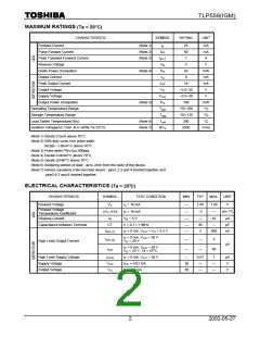
MAXIMUM RATINGS (Ta = 25°C)
CHARACTERISTIC
SYMBOL
RATING
UNIT
Forward Current
(Note 1)
(Note 2)
(Note 3)
I
25
50
mA
mA
A
F
Pulse Forward Current
Peak Transient Forward Current
Reverse Voltage
I
FP
I
1
FPT
V
P
5
V
R
D
Diode Power Dissipation
Output Current
(Note 4)
45
mW
mA
mA
V
I
8
O
Peak Output Current
I
16
OP
Output Voltage
V
−0.5~20
−0.5~30
100
O
Supply Voltage
V
V
CC
Output Power Dissipation
Operating Temperature Range
Storage Temperature Range
Lead Solder Temperature(10s)
Isolation Voltage(AC,1min.,R.H.≤60%,Ta=25°C)
(Note 5)
P
mW
O
T
−55~100
−55~125
260
°C
°C
opr
T
T
stg
(Note 6)
(Note 7)
°C
Vrms
sol
BV
2500
S
(Note 1) Derate 0.5mA above 70°C.
(Note 2) 50% duty cycle,1ms pulse width.
Derate –1.0mA/°C above 70°C.
(Note 3) Pulse width PW≤1µs,300pps.
(Note 4) Derate 0.9mW/°C above 70°C.
(Note 5) Derate 2mW/°C above 70°C.
(Note 6) Soldering portion of lead : up to 2mm from the body of the device.
(Note 7) Device considerd a two terminal device : pins1,2,3 and 4 shorted together and
pins5,6,7 and 8 shorted together.
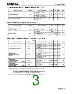
ELECTRICAL CHARACTERISTICS (Ta = 25℃)
CHARACTERISTIC
Forward Voltage
SYMBOL
TEST CONDITION
= 16 mA
MIN.
TYP.
MAX. UNIT
V
I
I
―
1.65
1.85
V
F
F
F
Forward Voltage
∆V /∆Ta
= 16 mA
= 5 V
−2
―
mV /°C
―
F
Temperature Coefficient
Reverse Current
I
V
―
45
3
10
―
µA
pF
nA
―
―
―
R
R
Capacitance between Terminal
CT
V = 0, f = 1 MHz
I
I
I
= 0 mA, V
= 0 mA, V
= V = 5.5 V
O
500
OH (1)
F
CC
CC
= 30 V
F
I
5
―
―
―
―
OH (2)
High Level Output Current
V
= 20 V
O
µA
I
= 0 mA, V
CC
= 30 V
F
I
50
OH
V
I
= 20 V, Ta = 70°C
O
High Level Supply Voltage
Supply Voltage
I
= 0 mA, V = 30 V
CC
0.01
―
1
µA
V
―
30
20
CCH
F
V
I
I
= 0.01 mA
CC
―
―
CC
Output Voltage
V
O
= 0.5 mA
V
―
O
2
2002-05-27

 TOSHIBA [ TOSHIBA ]