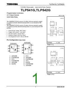
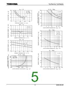
TLP541G, TLP542G
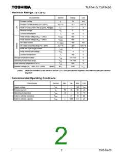
Maximum Ratings (Ta = 25°C)
Characteristic
Symbol
Rating
Unit
mA
Forward current
I
70
-0.7
1
F
Forward current derating (Ta ≥ 25°C)
Peak forward current (100 µs pulse, 100 pps)
Reverse voltage
∆I / °C
F
mA / °C
I
A
V
FP
V
5
R
Junction temperature
T
125
400
400
150
-2.0
2
°C
V
j
Peak forward voltage (R
Peak reverse voltage (R
On-state current
= 27kΩ)
= 27kΩ)
V
V
GK
DRM
RRM
V
GK
I
mA
mA / °C
A
T (RMS)
On-state current derating (Ta ≥ 25°C)
Peak one cycle surge current
Peak reverse gate voltage
Junction temperature
∆I / °C
T
I
TSM
V
-5
V
GM
T
100
-55~125
-30~100
260
2500
°C
°C
°C
°C
j
Storage temperature range
T
stg
opr
Operating temperature range
T
Lead soldering temperature (10 s)
Isolation voltage (AC, 1 min., R.H. ≤ 60%)
T
sol
(Note)
BV
V
rms
S
(Note) Device considered a two terminal device: LED side pins shorted together and detector side pins shorted
together.
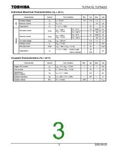
Recommended Operating Conditions
Characteristic
Symbol
Min.
Typ.
Max.
Unit
Supply voltage
Forward current
V
―
10
―
16
120
25
V
ac
AC
I
mA
°C
F
Operating temperature
Gate to cathode resistance
Gate to cathode capacity
T
-30
―
―
85
opr
R
27
33
kΩ
µF
GK
GK
C
―
0.01
0.1
2
2002-09-25

 TOSHIBA [ TOSHIBA ]