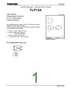
TLP124
Current Transfer Ratio
Current Transfer Ratio (min.)
Ta = 25°C Ta = −25~75°C
= 1mA = 0.5mA = 1mA
Marking Of
Classification
Classification
I
I
I
F
F
F
V
= 0.5V
V
= 1.5V
V
= 0.5V
CE
200%
100%
CE
100%
50%
CE
100%
50%
Rank BV
Standard
BV
BV, Blank
(Note) Application type name for certification test, please use standard product type name, i. e.
TLP124 (BV): TLP124
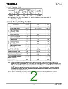
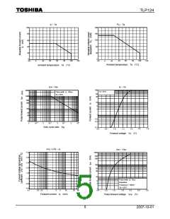
Absolute Maximum Ratings (Ta = 25°C)
Characteristic
Forward current
Symbol
Rating
Unit
I
50
mA
F
Forward current derating
ΔI / °C
F
−0.7 (Ta ≥ 53°C)
mA / °C
Peak forward current
(100μs pulse, 100pps)
I
1
A
FP
Reverse voltage
V
5
125
80
7
V
°C
V
R
Junction temperature
Collector−emitter voltage
Emitter−collector voltage
Collector current
T
j
V
V
CEO
ECO
V
I
50
mA
C
Peak collector current
(10ms pulse, 100pps)
I
100
150
−1.5
mA
mW
CP
Power dissipation
P
C
Power dissipation derating
(Ta ≥ 25°C)
ΔP / °C
mA / °C
C
Junction temperature
T
125
−55~125
−55~100
260
°C
°C
j
Storage temperature range
Operating temperature range
Lead soldering temperature (10s)
Total package power dissipation
T
stg
opr
T
°C
T
°C
sol
P
200
mW
T
Total package power dissipation
derating (Ta ≥ 25°C)
ΔP / °C
−2.0
mW / °C
Vrms
T
Isolation voltage
BV
3750
S
(AC, 1min., R.H. ≤ 60%)
(Note 1)
Note: Using continuously under heavy loads (e.g. the application of high temperature/current/voltage and the
significant change in temperature, etc.) may cause this product to decrease in the reliability significantly even
if the operating conditions (i.e. operating temperature/current/voltage, etc.) are within the absolute maximum
ratings.
Please design the appropriate reliability upon reviewing the Toshiba Semiconductor Reliability Handbook
(“Handling Precautions”/“Derating Concept and Methods”) and individual reliability data (i.e. reliability test
report and estimated failure rate, etc).
(Note 1) Device considered a two terminal device: Pins1, 3 shorted together and pins 4, 6 shorted together.
2
2007-10-01

 TOSHIBA [ TOSHIBA ]