TLP109
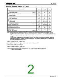
Absolute Maximum Ratings (Ta = 25°C)
Characteristic
Symbol
Rating
Unit
Forward current
Pulse forward current
Peak transient forward current
Reverse voltage
(Note 1)
(Note 2)
(Note 3)
I
20
mA
mA
A
F
I
40
FP
I
1
5
FPT
V
V
R
Output current
I
8
mA
mA
V
O
Peak output current
I
16
OP
Supply voltage
V
−0.5 to 30
−0.5 to 20
100
CC
Output voltage
V
V
O
O
Output power dissipation
Operating temperature range
Storage temperature range
Lead solder temperature (10 sec.)
Isolation Voltage
(Note 4)
P
mW
°C
°C
°C
T
opr
−55 to 100
−55 to 125
260
T
stg
sol
T
BV
3750
Vrms
S
(AC,1 min., R.H.≤ 60°%)
(Note 5)
Note: Using continuously under heavy loads (e.g. the application of high temperature/current/voltage and the
significant change in temperature, etc.) may cause this product to decrease in the reliability significantly even
if the operating conditions (i.e. operating temperature/current/voltage, etc.) are within the absolute maximum
ratings.
Please design the appropriate reliability upon reviewing the Toshiba Semiconductor Reliability Handbook
(“Handling Precautions”/“Derating Concept and Methods”) and individual reliability data (i.e. reliability test
report and estimated failure rate, etc).
(Note 1) Derate 0.36 mA / °C above 70°C.
(Note 2) 50% duty cycle, 1 ms pulse width. Derate 0.72 mA / °C above 70°C.
(Note 3) Pulse width ≤ 1 μs, 300 pps.
(Note 4) Derate 1.8 mW / °C above 70°C.
(Note 5) Device considered a two−terminal device: Pins 1 and 3 shorted together, and pins 4,
5 and 6 shorted together.
2
2009-04-01

 TOSHIBA [ TOSHIBA ]