TK7P60W
6. Electrical Characteristics
6.1. Static Characteristics (Ta = 25 unless otherwise specified)
Characteristics
Gate leakage current
Symbol
Test Condition
Min
Typ.
Max
Unit
IGSS
IDSS
VGS = ±30 V, VDS = 0 V
±1
10
µA
Drain cut-off current
VDS = 600 V, VGS = 0 V
Drain-source breakdown voltage
Gate threshold voltage
V(BR)DSS ID = 10 mA, VGS = 0 V
600
2.7
V
Vth
VDS = 10 V, ID = 0.35 mA
VGS = 10 V, ID = 3.5 A
3.7
0.6
Drain-source on-resistance
RDS(ON)
0.5
Ω
6.2. Dynamic Characteristics (Ta = 25 unless otherwise specified)
Characteristics
Input capacitance
Symbol
Test Condition
Min
Typ.
Max
Unit
pF
Ciss
Crss
Coss
Co(er)
rg
VDS = 300 V, VGS = 0 V, f = 1 MHz
25
490
1.7
13
Reverse transfer capacitance
Output capacitance
Effective output capacitance
Gate resistance
VDS = 0 to 400 V, VGS = 0 V
VDS = OPEN, f = 1 MHz
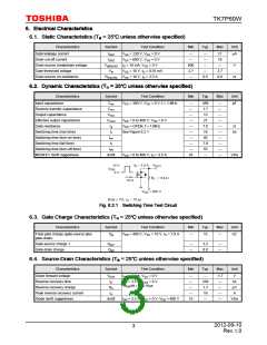
See Figure 6.2.1
21
7.0
18
Ω
Switching time (rise time)
Switching time (turn-on time)
Switching time (fall time)
Switching time (turn-off time)
MOSFET dv/dt ruggedness
tr
ns
ton
40
tf
7.0
55
toff
dv/dt
VDD = 0 to 400 V, ID = 3.5 A
V/ns
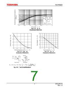
Fig. 6.2.1 Switching Time Test Circuit
6.3. Gate Charge Characteristics (Ta = 25 unless otherwise specified)
Characteristics
Symbol
Qg
Test Condition
Min
Typ.
15
Max
Unit
nC
Total gate charge (gate-source plus
gate-drain)
VDD ≈ 400 V, VGS = 10 V, ID = 7.0 A
Gate-source charge 1
Gate-drain charge
Qgs1
Qgd
3.2
8.0
6.4. Source-Drain Characteristics (Ta = 25 unless otherwise specified)
Characteristics
Diode forward voltage
Symbol
Test Condition
IDR = 7.0 A, VGS = 0 V
Min
Typ.
Max
Unit
VDSF
trr
15
230
1.7
16
-1.7
V
ns
Reverse recovery time
IDR = 3.5 A, VGS = 0 V
-dIDR/dt = 100 A/µs
Reverse recovery charge
Peak reverse recovery current
Diode dv/dt ruggedness
Qrr
µC
A
Irr
dv/dt
IDR = 3.5 A, VGS = 0 V, VDD = 400 V
V/ns
2012-09-10
Rev.1.0
3

 TOSHIBA [ TOSHIBA ]