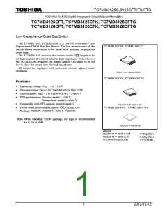
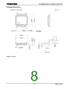
TC7MB3125C,3126CFT/FK/FTG
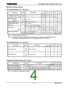
Electrical Characteristics
DC Characteristics (Ta = −40~85°C)
Typ.
Characteristics
Symbol
Test Condition
Min
Max
Unit
V
V
(V)
CC
“H” level
V
IH
⎯
⎯
4.0~5.5
4.0~5.5
2.0
⎯
⎯
⎯
Input voltage
( OE , OE)
“ L ” l e v e l
V
⎯
0.8
IL
Input leakage current
( OE , OE)
I
V
= 0~5.5 V
4.0~5.5
0
⎯
⎯
⎯
⎯
⎯
⎯
±1.0
10
μA
μA
μA
IN
IN
Power-off leakage current
Off-state leakage current
(switch off)
I
OE , OE, A, B = 0~5.5 V
A, B = 0~5.5 V,
OFF
I
4.0~5.5
±1.0
SZ
OE = V (3125C),OE=GND(3126C)
CC
V
= 0 V
I
= 30 mA
(Note1)
4.5
4.5
4.0
5.5
5.5
⎯
⎯
⎯
⎯
⎯
3
5
7
15
20
10
500
IS
IS
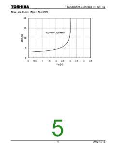
On resistance
R
Ω
ON
(Note2)
V
IS
= 2.4 V
I
IS
= 15 mA
(Note1)
9
Quiescent supply current
I
V
V
= V
CC
or GND, I
OUT
= 0 A
⎯
⎯
μA
μA
CC
IN
ΔI
CC
= 3.4V (one input)
IN
Note1: All typical values are at Ta=25°C.
Note2: Measured by the voltage drop between A and B pins at the indicated current through the switch.
On resistance is determined by the lower of the voltages on the two (A or B) pins.
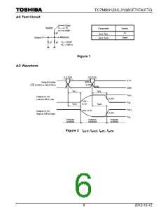
AC Characteristics (Ta = −40~85°C)
Characteristics
Symbol
Test Condition
Min
Max
6
Unit
ns
V
(V)
CC
t
pZL
Output enable time
Figure 1, Figure 2
4.5
⎯
t
pZH
t
pLZ
Output disable time
Figure 1, Figure 2
4.5
⎯
6
ns
t
pHZ
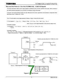
Capacitive Characteristics (Ta = 25°C)
Characteristics
Symbol
Test Condition
Typ.
Unit
V
CC
(V)
Control pin input capacitance
Switch OFF terminal capacitance
Switch ON terminal capacitance
C
V
V
V
=0 V
(Note)
5.0
5.0
5.0
5
4
7
pF
pF
pF
IN
I/O
I/O
IN
C
C
=0V, OE =Vcc(3125C), OE=GND(3126C) (Note)
I/O
=0V, OE =GND(3125C),OE=Vcc(3126C) (Note)
I/O
Note: This parameter is guaranteed by design
4
2012-12-12
图片预览")
 TOSHIBA [ TOSHIBA ]